
Datasheet


Data Sheet 10 Rev 1.0, 2012-09-01
ITS41k0S-ME-N
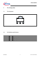
Application Information
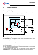
6.2 Special features
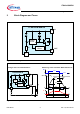
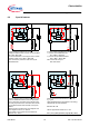
Figure 5 Special Feature descriptions
Energy stored in the load inductance is given by :
E
L
= I
L
²*L/2
While demagnetizing the load inductance the energy
dissipated by the Power -DMOS is:
E
AS
= E
S
+ E
L
–E
R
With an approximate solution for R
L
> 0Ω:
E
AS
= (I
L
*L) / (2*R
L
)*(V
S
+V
DSCL
)*ln((1+(I
L
*R
L
) / V
DSCL
)
When an inductive load is switched off a current path
must be established until the current is sloped down
to zero (all energy removed from the inductive load ).
For that purpose the series combination ZD 2 and D1
is connceted between Gate and Drain of the power
DMOS.
When the device is switched off, the voltage at OUT
turns negative until V
DSCL
is reached.
The Voltage on the incutive load is the difference
between V
DSCL
and V
S
.
If reverse Voltage is applied to the device :
1.) Current via Load Resistance RL :
I
Rev1
= (V
REV
–V
FM1
) / R
L
2.) Current via Input Resistance RIN:
I
REV2
= (V
REV
–V
FZD1
) / R
IN
Both currents will sum up to:
I
REV
= I
REV1
+ I
REV2
If Over-Voltage is applied to the V
S
-Pin:
Voltage is limited to VZD1; Current can be calculated :
I
ZD1
= (V
S
–V
ZD1
) / R
IN
In case of ESD Pulse on the input pin there is in both
polarities a peak current I
INpeak
~ V
ESD
/ R
IN
The control unit is protected in both cases by the
Zenerdiode ZD1
3
ITS41k0S-ME-N
1
Control
circuit
R
IN
2, 4
Temperature
Sensor
IN
OUT
V
S
3
ITS41k0S-ME-N
1
Control
circuit
R
IN
Temperature
Sensor
IN
OUT
V
S
Z
L
2, 4
I
REV1
I
REV2
V
REV
3
ITS41k0S-ME-N
1
Control
circuit
R
IN
Temperature
Sensor
IN
OUT
V
S
L
L
2, 4
I
L
V
Batt
V
DSCL
V
OUT
3
ITS41k0S-ME-N
1
Control
circuit
R
IN
Temperature
Sensor
IN
OUT
V
S
L
L
2, 4
E
R
R
L
t
ON
OFF
E
L
E
Batt
E
Load
Z
L
V
Batt
V
DS
V
OUT
V
ESD
t
ON
OFF
ZD
1
ZD
2
D
1
M
1
ZD
1
ZD
2
D
1
M
1
ZD
1
ZD
2
D
1
M
1
ZD
1
ZD
2
D
1
M
1
V
DSCL
I
REV
V
FM1
V
FZD1