
Datasheet

IRLR/U024NPbF
2 www.irf.com
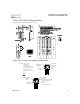
S
D
G
Parameter Min. Typ. Max. Units Conditions
I
S
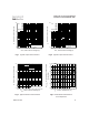
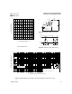
Continuous Source Current MOSFET symbol
(Body Diode)
––– –––
showing the
I
SM
Pulsed Source Current integral reverse
(Body Diode)
––– –––
p-n junction diode.
V
SD
Diode Forward Voltage ––– ––– 1.3 V T
J
= 25°C, I
S
= 11A, V
GS
= 0V
t
rr
Reverse Recovery Time ––– 60 90 ns T
J
= 25°C, I
F
= 11A
Q
rr
Reverse RecoveryCharge ––– 130 200 nC di/dt = 100A/µs
t
on
Forward Turn-On Time Intrinsic turn-on time is negligible (turn-on is dominated by L
S
+L
D
)
Source-Drain Ratings and Characteristics
17
72
A
V
DD
= 25V, starting T
J
= 25°C, L = 790µH
R
G
= 25Ω, I
AS
= 11A. (See Figure 12)
Repetitive rating; pulse width limited by
max. junction temperature. (See fig. 11)
Pulse width ≤ 300µs; duty cycle ≤ 2%.
Uses IRLZ24N data and test conditions.
This is applied for I-PAK, L
S
of D-PAK is measured between
lead and center of die contact
I
SD
≤ 11A, di/dt ≤ 290A/µs, V
DD
≤ V
(BR)DSS
,
T
J
≤ 175°C
Notes:
Parameter Min. Typ. Max. Units Conditions
V
(BR)DSS
Drain-to-Source Breakdown Voltage 55 ––– ––– V V
GS
= 0V, I
D
= 250µA
∆V
(BR)DSS
/∆T
J
Breakdown Voltage Temp. Coefficient ––– 0.061 ––– V/°C Reference to 25°C, I
D
= 1mA
––– ––– 0.065 V
GS
= 10V, I
D
= 10A
––– ––– 0.080 Ω V
GS
= 5.0V, I
D
= 10A
––– ––– 0.110 V
GS
= 4.0V, I
D
= 9.0A
V
GS(th)
Gate Threshold Voltage 1.0 ––– 2.0 V V
DS
= V
GS
, I
D
= 250µA
g
fs
Forward Transconductance 8.3 ––– ––– S V
DS
= 25V, I
D
= 11A
––– ––– 25
µA
V
DS
= 55V, V
GS
= 0V
––– ––– 250 V
DS
= 44V, V
GS
= 0V, T
J
= 150°C
Gate-to-Source Forward Leakage ––– ––– 100
nA
V
GS
= 16V
Gate-to-Source Reverse Leakage ––– ––– -100 V
GS
= -16V
Q
g
Total Gate Charge ––– ––– 15 I
D
= 11A
Q
gs
Gate-to-Source Charge ––– ––– 3.7 nC V
DS
= 44V
Q
gd
Gate-to-Drain ("Miller") Charge ––– ––– 8.5 V
GS
= 5.0V, See Fig. 6 and 13
t
d(on)
Turn-On Delay Time ––– 7.1 ––– V
DD
= 28V
t
r
Rise Time ––– 74 –––
ns
I
D
= 11A
t
d(off)
Turn-Off Delay Time ––– 20 ––– R
G
= 12Ω, V
GS
= 5.0V
t
f
Fall Time ––– 29 ––– R
D
= 2.4Ω, See Fig. 10
Between lead,
6mm (0.25in.)
from package
and center of die contact
C
iss
Input Capacitance ––– 480 ––– V
GS
= 0V
C
oss
Output Capacitance ––– 130 ––– pF V
DS
= 25V
C
rss
Reverse Transfer Capacitance ––– 61 ––– ƒ = 1.0MHz, See Fig. 5
Electrical Characteristics @ T
J
= 25°C (unless otherwise specified)
nH
I
GSS
S
D
G
L
S
Internal Source Inductance ––– 7.5 –––
R
DS(on)
Static Drain-to-Source On-Resistance
L
D
Internal Drain Inductance 4.5
I
DSS
Drain-to-Source Leakage Current