
Datasheet

IRLR/U3114ZPbF
2 www.irf.com
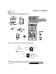
S
D
G
S
D
G
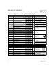
El
ectr
i
ca
l Ch
aracter
i
st
i
cs
@ T
J
=
2
5
°C (
un
l
ess
ot
h
erw
i
se
spec
ifi
e
d)
Parameter Min. T
y
p. Max. Units
V
(BR)DSS
Drain-to-Source Breakdown Volta
g
e40––––––V
∆V
(BR)DSS
/
∆T
J
Breakdown Volta
g
e Temp. Coefficient ––– 0.032 ––– V/°C
R
DS(on)
Static Drain-to-Source On-Resistance ––– 3.9 4.9
m
Ω
––– 5.2 6.5
V
GS(th)
Gate Threshold Volta
g
e 1.0 ––– 2.5 V
g
fs Forward Transconductance 98 ––– ––– S
I
DSS
Drain-to-Source Leaka
g
e Current ––– ––– 20 µA
––– ––– 250
I
GSS
Gate-to-Source Forward Leaka
g
e ––– ––– 100 nA
Gate-to-Source Reverse Leaka
g
e––––––-100
Q
g
Total Gate Char
g
e ––– 40 56
Q
gs
Gate-to-Source Char
g
e–––12–––nC
Q
gd
Gate-to-Drain ("Miller") Char
g
e–––18–––
t
d(on)
Turn-On Dela
y
Time ––– 25 –––
t
r
Rise Time ––– 140 –––
t
d(off)
Turn-Off Dela
y
Time ––– 33 ––– ns
t
f
Fall Time ––– 50 –––
L
D
Internal Drain Inductance ––– 4.5 ––– Between lead,
nH 6mm (0.25in.)
L
S
Internal Source Inductance ––– 7.5 ––– from packa
g
e
and center of die contact
C
iss
Input Capacitance ––– 3810 –––
C
oss
Output Capacitance ––– 650 –––
C
rss
Reverse Transfer Capacitance ––– 350 ––– pF
C
oss
Output Capacitance ––– 2390 –––
C
oss
Output Capacitance ––– 580 –––
C
oss
eff.
Effective Output Capacitance ––– 820 –––
Source-Drain Ratin
g
s and Characteristics
Parameter Min. T
y
p. Max. Units
I
S
Continuous Source Current ––– ––– 130
(Body Diode) A
I
SM
Pulsed Source Current ––– ––– 500
(
Bod
y
Diode
)
V
SD
Diode Forward Volta
g
e––––––1.3V
t
rr
Reverse Recover
y
Time –––3045ns
Q
rr
Reverse Recover
y
Char
g
e ––– 27 41 nC
t
on
Forward Turn-On Time
Intrinsic turn-on time is negligible (turn-on is dominated by LS+LD)
V
GS
= 4.5V, I
D
= 42A
V
GS
= 16V
V
GS
= -16V
V
DS
= 20V
V
DS
= 10V, I
D
= 42A
I
D
= 42A
Conditions
V
GS
= 4.5V
V
GS
= 0V
V
DS
= 25V
ƒ = 1.0MHz
V
GS
= 0V, V
DS
= 1.0V, ƒ = 1.0MHz
V
GS
= 0V, V
DS
= 32V, ƒ = 1.0MHz
V
GS
= 0V, V
DS
= 0V to 32V
MOSFET symbol
showing the
integral reverse
p-n junction diode.
T
J
= 25°C, I
S
= 42A, V
GS
= 0V
T
J
= 25°C, I
F
= 42A, V
DD
= 20V
di/dt = 100A/µs
Conditions
V
GS
= 0V, I
D
= 250µA
Reference to 25°C, I
D
= 1mA
V
GS
= 10V, I
D
= 42A
V
DS
= V
GS
, I
D
= 100µA
V
DS
= 40V, V
GS
= 0V
V
DS
= 40V, V
GS
= 0V, T
J
= 125°C
V
GS
= 4.5V
V
DD
= 20V
I
D
= 42A
R
G
= 3.7Ω