
Datasheet

IRLML9303TRPbF
2 www.irf.com
G
D
S
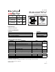
Electric Characteristics @ T
J
= 25°C (unless otherwise specified)
Symbol
Parameter
Min.
Typ.
Max.
Units
V
(BR)DSS
Drain-to-Source Breakdown Voltage -30 ––– ––– V
V
(BR)DSS
/
T
J
Breakdown Voltage Temp. Coefficient ––– -3.7 ––– mV/°C
––– 135 165
––– 220 270
V
GS(th)
Gate Threshold Voltage -1.3 ––– -2.4 V
I
DSS
––– ––– 1.0
––– ––– 150
I
GSS
Gate-to-Source Forward Leakage ––– ––– -100
Gate-to-Source Reverse Leakage ––– ––– 100
R
G
Internal Gate Resistance ––– 21 –––
gfs Forward Transconductance 2.3 ––– ––– S
Q
g
Total Gate Charge ––– 2.0 –––
Q
gs
Gate-to-Source Charge ––– 0.57 –––
Q
gd
Gate-to-Drain ("Miller") Charge ––– 1.2 –––
t
d(on)
Turn-On Delay Time ––– 7.5 –––
t
r
Rise Time –––14–––
t
d(off)
Turn-Off Delay Time ––– 9.0 –––
t
f
Fall Time ––– 8.6 –––
C
iss
Input Capacitance ––– 160 –––
C
oss
Output Capacitance ––– 39 –––
C
rss
Reverse Transfer Capacitance ––– 25 –––
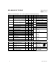
Source - Drain Ratings and Characteristics
Symbol
Parameter
Min.
Typ.
Max.
Units
I
S
Continuous Source Current
(Body Diode)
I
SM
Pulsed Source Current
(Body Diode)
V
SD
Diode Forward Voltage ––– ––– -1.2 V
t
rr
Reverse Recovery Time ––– 12 18 ns
Q
rr
Reverse Recovery Charge ––– 5.3 8.0 nC
––– –––
––– –––
pF
A
-1.3
-12
V
DD
=-15V
nA
nC
ns
V
DS
= V
GS
, I
D
= -10μA
V
DS
= -24V, V
GS
= 0V
V
DS
= -24V, V
GS
= 0V, T
J
= 125°C
R
DS(on)
V
GS
= -4.5V, I
D
=
-1.8A
Static Drain-to-Source On-Resistance
Drain-to-Source Leakage Current μA
m
Conditions
V
GS
= 0V, I
D
= -250μA
Reference to 25°C, I
D
= -1mA
V
GS
= -10V, I
D
= -2.3A
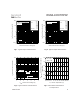
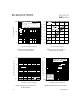
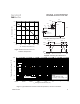
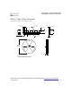
MOSFET symbol
showing the
V
DS
=-15V
Conditions
V
GS
= -4.5V
V
GS
= 0V
V
DS
= -25V
ƒ = 1.0KHz
R
G
= 6.8
V
GS
= -4.5V
di/dt = 100A/μs
V
GS
= -20V
V
GS
= 20V
T
J
= 25°C, I
S
= -1.3A, V
GS
= 0V
integral reverse
p-n junction diode.
V
DS
= -10V, I
D
=-2.3A
I
D
= -2.3A
I
D
= -1.0A
T
J
= 25°C, V
R
= -24V, I
F
=-1.3A