
Datasheet

IRLL3303
www.irf.com 5
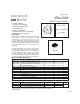
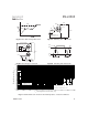
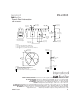
+
-
V
DS
10V
Pulse Width ≤ 1 µs
Duty Factor ≤ 0.1 %
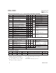
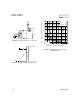
R
D
V
GS
V
DD
R
G
D.U.T.
10V
Q
G
Q
GS
Q
GD
V
G
Charge
D.U.T.
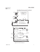
V
DS
I
D
I
G
3mA
V
GS
.3µF
50KΩ
.2µF
12V
Current Regulator
Same Type as D.U.T.
Current Sampling Resistors
+
-
V
DS
90%
10%
V
GS
t
d(on)
t
r
t
d(off)
t
f
Fig 10b. Switching Time Waveforms
Fig 10a. Switching Time Test Circuit
Fig 9a. Basic Gate Charge Waveform
Fig 9b. Gate Charge Test Circuit
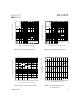
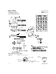
0.01
0.1
1
10
100
1000
0.00001 0.0001 0.001 0.01 0.1 1 10 100 1000 10000
t , Rectangular Pulse Duration (sec)
1
D = 0.50
0.01
0.02
0.05
0.10
0.20
S ING LE PULS E
(THERMAL RESPONSE)
A
Thermal Response (Z )
thJA
P
t
2
1
t
DM
Notes:
1. Duty factor D = t / t
2. Peak T = P x Z + T
1
2
J
DM
thJA
A
Fig 11. Maximum Effective Transient Thermal Impedance, Junction-to-Ambient