
Datasheet

IRLL3303
2 www.irf.com
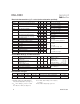
Parameter Min. Typ. Max. Units Conditions
V
(BR)DSS
Drain-to-Source Breakdown Voltage 30 ––– ––– V V
GS
= 0V, I
D
= 250µA
∆V
(BR)DSS
/∆T
J
Breakdown Voltage Temp. Coefficient ––– 0.034 ––– V/°C Reference to 25°C, I
D
= 1mA
––– ––– 0.031 V
GS
= 10V, I
D
= 4.6A
––– ––– 0.045 V
GS
= 4.5V, I
D
= 2.3A
V
GS(th)
Gate Threshold Voltage 1.0 ––– ––– V V
DS
= V
GS
, I
D
= 250µA
g
fs
Forward Transconductance 5.5 ––– ––– S V
DS
= 10V, I
D
= 2.3A
––– ––– 25 V
DS
= 30V, V
GS
= 0V
––– ––– 250 V
DS
= 24V, V
GS
= 0V, T
J
= 125°C
Gate-to-Source Forward Leakage ––– ––– -100 V
GS
= -16V
Gate-to-Source Reverse Leakage ––– ––– 100 V
GS
= 16V
Q
g
Total Gate Charge ––– 34 50 I
D
= 4.6A
Q
gs
Gate-to-Source Charge ––– 4.4 6.5 nC V
DS
= 24V
Q
gd
Gate-to-Drain ("Miller") Charge ––– 10 16 V
GS
= 10V, See Fig. 6 and 9
t
d(on)
Turn-On Delay Time ––– 7.2 ––– V
DD
= 15V
t
r
Rise Time ––– 22 ––– I
D
= 4.6A
t
d(off)
Turn-Off Delay Time ––– 33 ––– R
G
= 6.2Ω
t
f
Fall Time ––– 28 ––– R
D
= 3.2Ω, See Fig. 10
C
iss
Input Capacitance ––– 840 ––– V
GS
= 0V
C
oss
Output Capacitance ––– 340 ––– pF V
DS
= 25V
C
rss
Reverse Transfer Capacitance ––– 170 ––– ƒ = 1.0MHz, See Fig. 5
Electrical Characteristics @ T
J
= 25°C (unless otherwise specified)
I
GSS
µA
Ω
R
DS(on)
Static Drain-to-Source On-Resistance
I
DSS
Drain-to-Source Leakage Current
nA
ns
Parameter Min. Typ. Max. Units Conditions
I
S
Continuous Source Current
––– –––
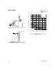
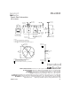
MOSFET symbol
(Body Diode) showing the
I
SM
Pulsed Source Current
––– –––
integral reverse
(Body Diode) p-n junction diode.
V
SD
Diode Forward Voltage ––– ––– 1.3 V T
J
= 25°C, I
S
= 4.6A, V
GS
= 0V
t
rr
Reverse Recovery Time ––– 65 98 ns T
J
= 25°C, I
F
= 4.6A
Q
rr
Reverse RecoveryCharge ––– 160 240 nC di/dt = 100A/µs
t
on
Forward Turn-On Time Intrinsic turn-on time is negligible (turn-on is dominated by L
S
+L
D
)
Source-Drain Ratings and Characteristics
A
37
0.91
Repetitive rating; pulse width limited by
max. junction temperature. ( See fig. 11 )
I
SD
≤ 4.6A, di/dt ≤ 110A/µs, V
DD
≤ V
(BR)DSS
,
T
J
≤ 150°C
Notes:
V
DD
= 15V, starting T
J
= 25°C, L = 13mH
R
G
= 25Ω, I
AS
= 4.6A. (See Figure 12)
Pulse width ≤ 300µs; duty cycle ≤ 2%.
Rev. # Parameters Old spec. New spec. Comments Revision Date
1V
GS(th)
(Max.) 2.5V No spec. Removed V
GS(th)
(Max). Specification 11/1/96
1V
GS
(Max.) ±20 ±16 Decrease V
GS
(Max). Specification 11/1/96
Specification changes