
Datasheet

IRLL2705
www.irf.com 5
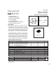
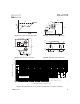
+
-
V
DS
10V
Pulse Width ≤ 1 µs
Duty Factor ≤ 0.1 %
R
D
V
GS
V
DD
R
G
D.U.T.
10V
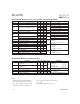
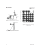
Q
G
Q
GS
Q
GD
V
G
Charge
D.U.T.
V
DS
I
D
I
G
3mA
V
GS
.3µF
50KΩ
.2µF
12V
Current Regulator
Same Type as D.U.T.
Current Sampling Resistors
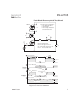
+
-
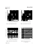
V
DS
90%
10%
V
GS
t
d(on)
t
r
t
d(off)
t
f
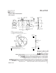
Fig 10b. Switching Time Waveforms
Fig 10a. Switching Time Test Circuit
Fig 9a. Basic Gate Charge Waveform
Fig 9b. Gate Charge Test Circuit
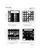
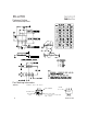
Fig 11. Maximum Effective Transient Thermal Impedance, Junction-to-Ambient
0.01
0.1
1
10
100
1000
0.00001 0.0001 0.001 0.01 0.1 1 10 100 1000 10000
t , Rectangular Pulse Duration (sec)
1
D = 0.50
0.01
0.02
0.05
0.10
0.20
SING LE PU LSE
(THERMAL RESPONSE)
A
Thermal Response (Z )
thJA
P
t
2
1
t
DM
Notes:
1. Duty factor D = t / t
2. Peak T = P x Z + T
1
2
J
DM
thJA
A