
Datasheet
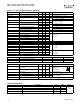

IRLHS2242TR/TR2PbF
6 www.irf.com
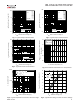
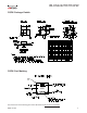
Fig 17a. Gate Charge Test Circuit
Fig 17b. Gate Charge Waveform
Vds
Vgs
Id
Vgs(th)
Qgs1
Qgs2QgdQgodr
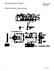
* Reverse Polarity of D.U.T for P-Channel
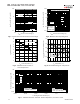
P.W.
Period
di/dt
Diode Recovery
dv/dt
Ripple ≤ 5%
Body Diode Forward Drop
Re-Applied
Voltage
Reverse
Recovery
Current
Body Diode Forward
Current
V
GS
=10V
V
DD
I
SD
Driver Gate Drive
D.U.T. I
SD
Waveform
D.U.T. V
DS
Waveform
Inductor Curent
D =
P. W .
Period
* V
GS
= 5V for Logic Level Devices
*
Inductor Current
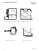
Circuit Layout Considerations
• Low Stray Inductance
• Ground Plane
• Low Leakage Inductance
Current Transformer
• di/dt controlled by R
G
• Driver same type as D.U.T.
• I
SD
controlled by Duty Factor "D"
• D.U.T. - Device Under Test
+
-
+
+
+
-
-
-
R
G
V
DD
D.U.T *
Fig 16. Diode Reverse Recovery Test Circuit for P-Channel HEXFET
®
Power MOSFETs
1K
VCC
DUT
0
L
S
20K
S