
Datasheet

IRLB8748PbF
2 www.irf.com
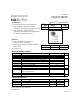
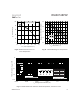
Static @ T
J
= 25°C (unless otherwise specified)
Parameter Min. T
y
p. Max. Units
BV
DSS
Drain-to-Source Breakdown Voltage
30 ––– ––– V
∆Β
V
DSS
/
∆
T
J
Breakdown Voltage Temp. Coefficient
––– 21 ––– mV/°C
R
DS(on)
Static Drain-to-Source On-Resistance
––– 3.8 4.8
––– 5.5 6.8
V
GS(th)
Gate Threshold Voltage
1.35 1.8 2.35 V
∆
V
GS(th)
/
∆
T
J
Gate Threshold Voltage Coefficient
––– -7.1 ––– mV/°C
I
DSS
Drain-to-Source Leakage Current
––– ––– 1.0
––– ––– 150
I
GSS
Gate-to-Source Forward Leakage
––– ––– 100
Gate-to-Source Reverse Leakage
––– ––– -100
gfs
Forward Transconductance
196 ––– ––– S
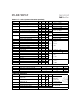
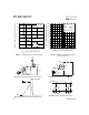
Q
g
Total Gate Charge
––– 15 23
Q
gs1
Pre-Vth Gate-to-Source Charge
––– 3.6 –––
Q
gs2
Post-Vth Gate-to-Source Charge
––– 2.2 ––– nC
Q
gd
Gate-to-Drain Charge
–––
5.9
–––
Q
godr
Gate Charge Overdrive
–––
3.9
–––
Q
sw Switch Charge (Q
gs2
+ Q
gd
)
–––
8.1
–––
Q
oss
Output Charge
–––
11
––– nC
R
G
Gate Resistance ––– 2.0 3.5
Ω
t
d(on)
Turn-On Delay Time
––– 14 –––
t
r
Rise Time
––– 96 –––
t
d(off)
Turn-Off Delay Time
––– 16 –––
t
f
Fall Time
––– 34 –––
C
iss
Input Capacitance
––– 2139 –––
C
oss
Output Capacitance
––– 464 –––
C
rss
Reverse Transfer Capacitance
––– 199 –––
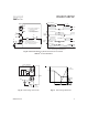
Avalanche Characteristics
Parameter Units
E
AS
Single Pulse Avalanche Energy
mJ
I
AR
Avalanche Current
A
E
AR
Repetitive Avalanche Energy
mJ
Diode Characteristics
Parameter Min. T
y
p. Max. Units
I
S
Continuous Source Current
––– –––
(Body Diode)
I
SM
Pulsed Source Current
––– –––
(Body Diode)
V
SD
Diode Forward Voltage
––– ––– 1.0 V
t
rr
Reverse Recovery Time
–––2335ns
Q
rr
Reverse Recovery Charge
––– 39 59 nC
t
on
Forward Turn-On Time
m
Ω
92
370
µA
nA
ns
pF
A
Typ.
–––
Conditions
7.5
Max.
114
32
ƒ = 1.0MHz
V
DS
= 24V, V
GS
= 0V
V
DS
= 24V, V
GS
= 0V, T
J
= 125°C
V
DS
= 15V, I
D
= 32A
V
DS
= V
GS
, I
D
= 50µA
V
DS
= 15V
V
GS
= 4.5V
Conditions
V
GS
= 0V, I
D
= 250µA
Reference to 25°C, I
D
= 1mA
V
GS
= 10V, I
D
= 40A
V
GS
= 4.5V, I
D
= 32A
V
GS
= 20V
V
GS
= -20V
–––
I
D
= 32A
V
GS
= 0V
V
DS
= 15V
R
G
= 1.8Ω
I
D
= 32A
V
DS
= 16V, V
GS
= 0V
V
DD
= 15V, V
GS
= 4.5V
Intrinsic turn-on time is negligible (turn-on is dominated by LS+LD)
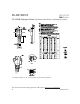
MOSFET symbol
–––
T
J
= 25°C, I
F
= 32A, V
DD
= 15V
di/dt = 200A/
µ
s
T
J
= 25°C, I
S
= 32A, V
GS
= 0V
showing the
integral reverse
p-n junction diode.