
Datasheet

IRL3302S
Repetitive rating; pulse width limited by
max. junction temperature.
I
SD
£ 23A, di/dt £ 97A/µs, V
DD
£ V
(BR)DSS
,
T
J
£ 150°C
Notes:
Starting T
J
= 25°C, L = 0.49mH
R
G
= 25W , I
AS
= 23A.
Pulse width £ 300µs; duty cycle £ 2%.
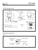
S
D
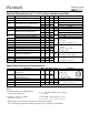
G
Parameter Min. Typ. Max. Units Conditions
I
S
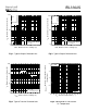
Continuous Source Current MOSFET symbol
(Body Diode)
––– –––
showing the
I
SM
Pulsed Source Current integral reverse
(Body Diode)
––– –––
p-n junction diode.
V
SD
Diode Forward Voltage ––– ––– 1.3 V T
J
= 25°C, I
S
= 23A, V
GS
= 0V
t
rr
Reverse Recovery Time ––– 62 94 ns T
J
= 25°C, I
F
= 23A
Q
rr
Reverse Recovery Charge ––– 110 160 nC di/dt = 100A/µs
t
on
Forward Turn-On Time Intrinsic turn-on time is negligible (turn-on is dominated by L
S
+L
D
)
Source-Drain Ratings and Characteristics
39
160
A
Parameter Min. Typ. Max. Units Conditions
V
(BR)DSS
Drain-to-Source Breakdown Voltage 20 ––– ––– V V
GS
= 0V, I
D
= 250µA
DV
(BR)DSS
/DT
J
Breakdown Voltage Temp. Coefficient ––– 0.022 ––– V/°C Reference to 25°C, I
D
= 1mA
––– ––– 0.023 V
GS
= 4.5V, I
D
= 23A
––– ––– 0.020
W
V
GS
= 7.0V, I
D
= 23A
V
GS(th)
Gate Threshold Voltage 0.70 ––– ––– V V
DS
= V
GS
, I
D
= 250µA
g
fs
Forward Transconductance 21 ––– ––– S V
DS
= 10V, I
D
= 23A
––– ––– 25
µA
V
DS
= 20V, V
GS
= 0V
––– ––– 250 V
DS
= 10V, V
GS
= 0V, T
J
= 150°C
Gate-to-Source Forward Leakage ––– ––– 100
nA
V
GS
= 10V
Gate-to-Source Reverse Leakage ––– ––– -100 V
GS
= -10V
Q
g
Total Gate Charge ––– ––– 31 I
D
= 23A
Q
gs
Gate-to-Source Charge ––– ––– 5.7 nC V
DS
= 16V
Q
gd
Gate-to-Drain ("Miller") Charge ––– ––– 13 V
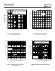
GS
= 4.5V, See Fig. 6
t
d(on)
Turn-On Delay Time ––– 7.2 ––– V
DD
= 10V
t
r
Rise Time ––– 110 –––
ns
I
D
= 23A
t
d(off)
Turn-Off Delay Time ––– 41 ––– R
G
= 9.5W, V
GS
= 4.5V
t
f
Fall Time ––– 89 ––– R
D
= 2.4W,
Between lead,
and center of die contact
C
iss
Input Capacitance ––– 1300 ––– V
GS
= 0V
C
oss
Output Capacitance ––– 520 ––– pF V
DS
= 15V
C
rss
Reverse Transfer Capacitance ––– 190 ––– ƒ = 1.0MHz, See Fig. 5
Electrical Characteristics @ T
J
= 25°C (unless otherwise specified)
R
DS(on)
Static Drain-to-Source On-Resistance
I
GSS
nH
L
S
Internal Source Inductance ––– 7.5 –––
I
DSS
Drain-to-Source Leakage Current
Uses IRL3302 data and test conditions
** When mounted on FR-4 board using minimum recommended footprint.
For recommended footprint and soldering techniques refer to application note #AN-994.