
Datasheet


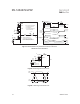

IRL1404Z/S/LPbF
2 www.irf.com
Notes:
Repetitive rating; pulse width limited by
max. junction temperature. (See fig. 11).
Limited by T
Jmax
, starting T
J
= 25°C,
L = 0.079mH, R
G
= 25Ω, I
AS
= 75A, V
GS
=10V.
Part not recommended for use above this value.
Pulse width ≤ 1.0ms; duty cycle ≤ 2%.
C
oss
eff. is a fixed capacitance that gives the same
charging time as C
oss
while V
DS
is rising from 0 to
80% V
DSS
.
Limited by T
Jmax
, see Fig.12a, 12b, 15, 16 for typical
repetitive avalanche performance.
This value determined from sample failure population. 100%
tested to this value in production.
This is only applied to TO-220AB package.
When mounted on 1" square PCB (FR-4 or G-10 Material).
For recommended footprint and soldering techniques
refer to application note #AN-994.
Calculated continuous current based on maximum allowable
junction temperature. Bond wire current limit is 120A. Note that
current limitations arising from heating of the device leads may
occur with some lead mounting arrangements.
All AC and DC test condition based on former Package limited
current of 75A.
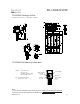
S
D
G
S
D
G
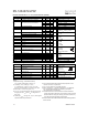
Electrical Characteristics @ T
J
= 25°C (unless otherwise specified)
Parameter Min. Typ. Max. Units
V
(BR)DSS
Drain-to-Source Breakdown Voltage 40 ––– ––– V
ΔV
(BR)DSS
/ΔT
J
Breakdown Voltage Temp. Coefficient ––– 0.034 ––– V/°C
––– 2.5 3.1
R
DS(on)
Static Drain-to-Source On-Resistance ––– ––– 4.7
mΩ
––– ––– 5.9
V
GS(th)
Gate Threshold Voltage 1.4 ––– 2.7 V
gfs Forward Transconductance 120 ––– ––– S
I
DSS
Drain-to-Source Leakage Current ––– ––– 20 μA
––– ––– 250
I
GSS
Gate-to-Source Forward Leakage ––– ––– 200 nA
Gate-to-Source Reverse Leakage ––– ––– -200
Q
g
Total Gate Charge ––– 75 110
Q
gs
Gate-to-Source Charge ––– 28 ––– nC
Q
gd
Gate-to-Drain ("Miller") Charge ––– 40 –––
t
d(on)
Turn-On Delay Time ––– 19 –––
t
r
Rise Time ––– 180 –––
t
d(off)
Turn-Off Delay Time ––– 30 ––– ns
t
f
Fall Time ––– 49 –––
L
D
Internal Drain Inductance ––– 4.5 ––– Between lead,
nH 6mm (0.25in.)
L
S
Internal Source Inductance ––– 7.5 ––– from package
and center of die contact
C
iss
Input Capacitance ––– 5080 –––
C
oss
Output Capacitance ––– 970 –––
C
rss
Reverse Transfer Capacitance ––– 570 ––– pF
C
oss
Output Capacitance ––– 3310 –––
C
oss
Output Capacitance ––– 870 –––
C
oss
eff. Effective Output Capacitance ––– 1280 –––
Source-Drain Ratings and Characteristics
Parameter Min. Typ. Max. Units
I
S
Continuous Source Current ––– –––
200
(Body Diode) A
I
SM
Pulsed Source Current ––– ––– 790
(Body Diode)
V
SD
Diode Forward Voltage ––– ––– 1.3 V
t
rr
Reverse Recovery Time ––– 26 39 ns
Q
rr
Reverse Recovery Charge ––– 18 27 nC
t
on
Forward Turn-On Time Intrinsic turn-on time is negligible (turn-on is dominated by LS+LD)
V
DS
= 40V, V
GS
= 0V, T
J
= 125°C
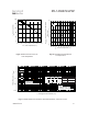
MOSFET symbol
showing the
integral reverse
p-n junction diode.
V
GS
= 16V
V
GS
= -16V
V
DS
= 32V
Conditions
V
GS
= 5.0V
I
D
= 75A
V
GS
= 0V
V
DS
= 25V
T
J
= 25°C, I
S
= 75A , V
GS
= 0V
T
J
= 25°C, I
F
= 75A , V
DD
= 20V
di/dt = 100A/μs
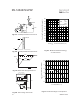
Conditions
V
GS
= 0V, I
D
= 250μA
Reference to 25°C, I
D
= 1mA
V
GS
= 10V, I
D
= 75A
V
DS
= V
GS
, I
D
= 250μA
V
DS
= 40V, V
GS
= 0V
V
GS
= 4.5V, I
D
= 40A
V
GS
= 5.0V, I
D
= 40A
V
GS
= 0V, V
DS
= 1.0V, ƒ = 1.0MHz
V
GS
= 0V, V
DS
= 32V, ƒ = 1.0MHz
V
GS
= 0V, V
DS
= 0V to 32V
V
GS
= 5.0V
V
DD
= 20V
I
D
= 75A
R
G
= 4.0Ω
V
DS
= 10V, I
D
= 75A
ƒ = 1.0MHz