
Datasheet


IRFR/U4615PbF
2 www.irf.com
S
D
G
Static @ T
J
= 25°C (unless otherwise specified)
Symbol Parameter Min. Typ. Max. Unit
s
V
(BR)DSS
Drain-to-Source Breakdown Volta
g
e 150 ––– ––– V
∆
V
(BR)DSS
/
∆
T
J
Breakdown Volta
g
e Temp. Coefficient ––– 0.19 ––– V/°C
R
DS(on)
Static Drain-to-Source On-Resistance ––– 34 42
m
Ω
V
GS(th)
Gate Threshold Volta
g
e 3.0 ––– 5.0 V
I
DSS
Drain-to-Source Leaka
g
e Current ––– ––– 20
––– ––– 250
I
GSS
Gate-to-Source Forward Leaka
g
e ––– ––– 100
Gate-to-Source Reverse Leaka
g
e ––– ––– -100
R
G
(
int
)
Internal Gate Resistance
–––
2.7 ––– Ω
Dynamic @ T
J
= 25°C (unless otherwise specified)
Symbol Parameter Min. Typ. Max. Unit
s
g
fs Forward Transconductance 35 ––– ––– S
Q
g
Total Gate Char
g
e ––– 26
Q
gs
Gate-to-Source Char
g
e ––– 8.6 –––
Q
gd
Gate-to-Drain ("Miller") Char
g
e ––– 9.0 –––
Q
sync
Total Gate Char
g
e Sync. (Q
g
- Q
gd
)
––– 17 –––
t
d(on)
Turn-On Delay Time ––– 15 –––
t
r
Rise Time ––– 35 –––
t
d(off)
Turn-Off Delay Time ––– 25 –––
t
f
Fall Time ––– 20 –––
C
iss
Input Capacitance ––– 1750 –––
C
oss
Output Capacitance ––– 155 –––
C
rss
Reverse Transfer Capacitance ––– 40 –––
C
oss
eff. (ER)
Effective Output Capacitance (Energy Related)
––– 179 –––
C
oss
eff. (TR)
Effective Output Capacitance (Time Related)
––– 382 –––
Diode Characteristics
Symbol Parameter Min. Typ. Max. Unit
s
I
S
Continuous Source Current
(Body Diode)
I
SM
Pulsed Source Current
(Body Diode)
V
SD
Diode Forward Volta
g
e ––– ––– 1.3 V
t
rr
Reverse Recovery Time ––– 70 –––
T
J
= 25°C V
R
= 100V,
––– 83 –––
T
J
= 125°C I
F
= 21A
Q
rr
Reverse Recovery Char
g
e ––– 177 –––
T
J
= 25°C
di
/
dt = 100A
/
µs
––– 247 –––
T
J
= 125°C
I
RRM
Reverse Recovery Current ––– 4.9 ––– A
T
J
= 25°C
t
on
Forward Turn-On Time Intrinsic turn-on time is ne
g
li
g
ible (turn-on is dominated by LS+LD)
ns
nC
33
140
µA
nA
nC
ns
pF
A
––– –––
––– –––
I
D
= 21A
R
G
= 7.3
Ω
V
GS
= 10V
V
DD
= 98V
I
D
= 21A, V
DS
=0V, V
GS
= 10V
T
J
= 25°C, I
S
= 21A, V
GS
= 0V
integral reverse
p-n junction diode.
Conditions
V
GS
= 0V, I
D
= 250µA
Reference to 25°C, I
D
= 5mA
V
GS
= 10V, I
D
= 21A
V
DS
= V
GS
, I
D
= 100µA
V
DS
= 150V, V
GS
= 0V
V
DS
= 150V, V
GS
= 0V, T
J
= 125°C
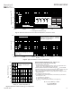
MOSFET symbol
showing the
V
DS
= 75V
Conditions
V
GS
= 10V
V
GS
= 0V
V
DS
= 50V
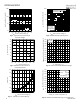
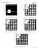
ƒ = 1.0MHz (See Fig.5)
V
GS
= 0V, V
DS
= 0V to 120V (See Fig.11)
V
GS
= 0V, V
DS
= 0V to 120V
Conditions
V
DS
= 50V, I
D
= 21A
I
D
= 21A
V
GS
= 20V
V
GS
= -20V