
Datasheet
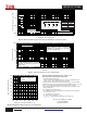

IRFS3107-7PPbF
www.irf.com © 2014 International Rectifier Submit Datasheet Feedback January 28, 20147
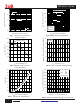
Fig 23a. Switching Time Test Circuit Fig 23b. Switching Time Waveforms
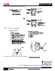
Fig 22b. Unclamped Inductive Waveforms
Fig 22a. Unclamped Inductive Test Circuit
t
p
V
(BR)DSS
I
AS
R
G
I
AS
0.01
Ω
t
p
D.U.T
L
V
DS
+
-
V
DD
DRIVER
A
15V
20V
V
GS
Fig 24a. Gate Charge Test Circuit
Fig 24b. Gate Charge Waveform
Vds
Vgs
Id
Vgs(th)
Qgs1
Qgs2 Qgd Qgodr
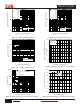
Fig 21. Peak Diode Recovery dv/dt Test Circuit for N-Channel
HEXFET
®
Power MOSFETs
Circuit Layout Considerations
• Low Stray Inductance
• Ground Plane
• Low Leakage Inductance
Current Transformer
P.W.
Period
di/dt
Diode Recovery
dv/dt
Ripple ≤ 5%
Body Diode Forward Drop
Re-Applied
Voltage
Reverse
Recovery
Current
Body Diode Forward
Current
V
GS
=10V
V
DD
I
SD
Driver Gate Drive
D.U.T. I
SD
Waveform
D.U.T. V
DS
Waveform
Inductor Curent
D =
P. W .
Period
* V
GS
= 5V for Logic Level Devices
*
+
-
+
+
+
-
-
-
R
G
V
DD
• dv/dt controlled by R
G
• Driver same type as D.U.T.
• I
SD
controlled by Duty Factor "D"
• D.U.T. - Device Under Test
D.U.T
Inductor Current
D.U.T.
V
DS
I
D
I
G
3mA
V
GS
.3µF
50KΩ
.2µF
12V
Current Regulator
Same Type as D.U.T.
Current Sampling Resistors
+
-
V
DS
90%
10%
V
GS
t
d(on)
t
r
t
d(off)
t
f
V
DS
Pulse Width ≤ 1 µs
Duty Factor ≤ 0.1 %
R
D
V
GS
R
G
D.U.T.
10V
+
-
V
DD
V
GS