
Datasheet

IRFP7430PbF
www.irf.com © 2015 International Rectifier Submit Datasheet Feedback February 19, 2015
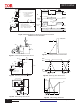
3
S
D
G
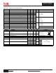
Dynamic @ T
J
= 25°C (unless otherwise specified)
Symbol Parameter Min. Typ. Max. Units
gfs Forward Transconductance 150 ––– ––– S
Q
g
Total Gate Charge ––– 300 460 nC
Q
gs
Gate-to-Source Charge ––– 77 –––
Q
gd
Gate-to-Drain ("Miller") Charge ––– 98 –––
Q
sync
Total Gate Charge Sync. (Q
g
- Q
gd
) ––– 202 –––
t
d(on)
Turn-On Delay Time ––– 32 ––– ns
t
r
Rise Time ––– 105 –––
t
d(off)
Turn-Off Delay Time ––– 160 –––
t
f
Fall Time ––– 100 –––
C
iss
Input Capacitance ––– 14240 ––– pF
C
oss
Output Capacitance ––– 2130 –––
C
rss
Reverse Transfer Capacitance ––– 1460 –––
C
oss
eff. (ER)
Effective Output Capacitance (Energy Related)
––– 2605 –––
C
oss
eff. (TR)
Effective Output Capacitance (Time Related)
––– 2920 –––
Diode Characteristics
Symbol Parameter Min. Typ. Max. Units
I
S
Continuous Source Current ––– –––
376
A
(Body Diode)
I
SM
Pulsed Source Current ––– ––– 1576 A
(Body Diode)
V
SD
Diode Forward Voltage ––– 0.86 1.2 V
dv/dt
Peak Diode Recovery
––– 2.7 ––– V/ns
t
rr
Reverse Recovery Time ––– 52 ––– ns T
J
= 25°C V
R
= 34V,
––– 52 ––– T
J
= 125°C I
F
= 100A
Q
rr
Reverse Recovery Charge ––– 97 ––– nC T
J
= 25°C
di/dt = 100A/μs
––– 97 ––– T
J
= 125°C
I
RRM
Reverse Recovery Current ––– 2.3 ––– A T
J
= 25°C
V
DS
= 10V, I
D
= 100A
V
DS
=20V
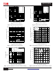
ƒ = 1.0 MHz
V
GS
= 0V, V
DS
= 0V to 32V
V
GS
= 0V, V
DS
= 0V to 32V
I
D
= 100A
V
GS
= 10V
V
GS
= 0V
V
DS
= 25V
Conditions
T
J
= 25°C, I
S
= 100A, V
GS
= 0V
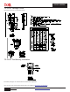
integral reverse
p-n junction diode.
MOSFET symbol
showing the
Conditions
T
J
= 175°C, I
S
= 100A, V
DS
= 40V
I
D
= 30A
R
G
= 2.7
Ω
V
GS
= 10V
V
DD
= 20V