
Datasheet

IRFP4868PbF
2 www.irf.com © 2012 International Rectifier October 30, 2012
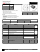
Static @ T
J
= 25°C (unless otherwise specified)
Symbol Parameter Min. Typ. Max. Units Conditions
V
(BR)DSS
Drain-to-Source Breakdown Voltage 300 ––– ––– V V
GS
= 0V, I
D
= 250µA
V
(BR)DSS
/T
J
Breakdown Voltage Temp. Coefficient ––– 0.29 ––– V/°C Reference to 25°C, I
D
= 5mA
R
DS(on)
Static Drain-to-Source On-Resistance ––– 25.5 32
m
V
GS
= 10V, I
D
= 42A
V
GS(th)
Gate Threshold Voltage 3.0 ––– 5.0 V V
DS
= V
GS
, I
D
= 250µA
I
DSS
Drain-to-Source Leakage Current ––– ––– 20 µA V
DS
= 300V, V
GS
= 0V
––– ––– 250
V
DS
= 300V, V
GS
= 0V, T
J
= 125°C
I
GSS
Gate-to-Source Forward Leakage ––– ––– 100 nA V
GS
= 20V
Gate-to-Source Reverse Leakage ––– ––– -100
V
GS
= -20V
R
G
Internal Gate Resistance ––– 1.1 –––
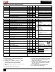
Dynamic @ T
J
= 25°C (unless otherwise specified)
Symbol Parameter Min. Typ. Max. Units Conditions
gfs Forward Transconductance 80 ––– ––– S V
DS
= 50V, I
D
= 42A
Q
g
Total Gate Charge ––– 180 270 nC I
D
= 42A
Q
gs
Gate-to-Source Charge ––– 60 –––
V
DS
=150V
Q
gd
Gate-to-Drain ("Miller") Charge ––– 57 –––
V
GS
= 10V
Q
sync
Total Gate Charge Sync. (Q
g
- Q
gd
) ––– 123 –––
I
D
= 42A, V
DS
=0V, V
GS
= 10V
t
d(on)
Turn-On Delay Time ––– 24 ––– ns V
DD
= 195V
t
r
Rise Time ––– 16 –––
I
D
= 42A
t
d(off)
Turn-Off Delay Time ––– 62 –––
R
G
= 1.0
t
f
Fall Time ––– 45 –––
V
GS
= 10V
C
iss
Input Capacitance ––– 10774 ––– pF V
GS
= 0V
C
oss
Output Capacitance ––– 612 –––
V
DS
= 50V
C
rss
Reverse Transfer Capacitance ––– 193 –––
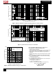
ƒ = 1.0 MHz, See Fig. 5
C
oss
eff. (ER) Effective Output Capacitance
(Energy Related)
––– 406 –––
V
GS
= 0V, V
DS
= 0V to 240V ,
See Fig. 11
C
oss
eff. (TR) Effective Output Capacitance
(Time Related)
––– 710 –––
V
GS
= 0V, V
DS
= 0V to 240V
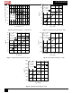
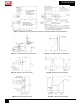
Diode Characteristics
Symbol Parameter Min. Typ. Max. Units Conditions
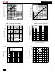
I
S
Continuous Source Current ––– ––– 70 A MOSFET symbol
(Body Diode) showing the
I
SM
Pulsed Source Current ––– ––– 280 A
integral reverse
(Body Diode) p-n junction diode.
V
SD
Diode Forward Voltage ––– ––– 1.3 V T
J
= 25°C, I
S
= 42A, V
GS
= 0V
t
rr
Reverse Recovery Time ––– 351 ––– ns T
J
= 25°C
––– 454 –––
T
J
= 125°C
Q
rr
Reverse Recovery Charge ––– 2520 ––– nC T
J
= 25°C
––– 3686 –––
T
J
= 125°C
I
RRM
Reverse Recovery Current ––– 16 ––– A T
J
= 25°C
t
on
Forward Turn-On Time Intrinsic turn-on time is negligible (turn-on is dominated by
LS+LD)
dv/dt Peak Diode Recovery ––– 7.3 ––– V/ns T
J
= 25°C, I
S
= 42A, V
DS
= 300V
Notes:
Repetitive rating; pulse width limited by max.
junction temperature.
Limited by T
Jmax
, starting T
J
= 25°C, L = 1.2mH
R
G
= 50, I
AS
= 42A, V
GS
=10V. Part not
recommended for use above this value.
ISD ≤ 42A, di/dt ≤ 1706A/µs, V
DD
≤ V
(BR)DSS
, T
J
≤
175°C.
Pulse width ≤ 400µs; duty cycle ≤ 2%.
Coss eff. (TR) is a fixed capacitance that gives
the same charging time as Coss while V
DS
is
rising from 0 to 80% V
DSS
.
Coss eff. (ER) is a fixed capacitance that gives
the same energy as Coss while V
DS
is rising
from 0 to 80% V
DSS
.
R
is measured at T
J
approximately 90°C.
R
JC
value shown is at time zero.
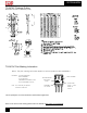
D
S
G
V
R
= 255V,
I
F
= 42A
di/dt = 100A/µs