
Datasheet


2 www.irf.com
IRFI4024H-117P
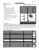
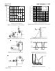
S
D
G
S
D
G
Notes:
Repetitive rating; pulse width limited by max. junction temperature.
Starting T
J
= 25°C, L = 0.25mH, R
G
= 25Ω, I
AS
= 7.7A.
Pulse width ≤ 400µs; duty cycle ≤ 2%.
R
θ
is measured at T
J
of approximately 90°C.
Specifications refer to single MosFET.
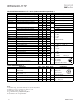
Electrical Characteristics @ T
J
= 25°C (unless otherwise specified)
g
Parameter Min. Typ. Max. Units
BV
DSS
Drain-to-Source Breakdown Voltage 55 ––– ––– V
∆ΒV
DSS
/
∆T
J
Breakdown Voltage Temp. Coefficient ––– 54 ––– mV/°C
R
DS(on)
Static Drain-to-Source On-Resistance ––– 48 60
mΩ
V
GS(th)
Gate Threshold Voltage 2.0 ––– 4.0 V
∆V
GS(th)
/
∆T
J
Gate Threshold Voltage Coefficient ––– -9.17 ––– mV/°C
I
DSS
Drain-to-Source Leakage Current ––– ––– 20 µA
––– ––– 250
I
GSS
Gate-to-Source Forward Leakage ––– ––– 200 nA
Gate-to-Source Reverse Leakage ––– ––– -200
g
fs
Forward Transconductance 6.5 ––– ––– S
Q
g
Total Gate Charge ––– 8.9 13
Q
gs1
Pre-Vth Gate-to-Source Charge ––– 1.6 –––
Q
gs2
Post-Vth Gate-to-Source Charge ––– 0.77 ––– nC
Q
gd
Gate-to-Drain Charge ––– 3.5 –––
Q
godr
Gate Charge Overdrive ––– 3.0 ––– See Fig. 6 and 15
Q
sw
Switch Charge (Q
gs2
+ Q
gd
)
––– 4.3 –––
R
G(int)
Internal Gate Resistance ––– 2.3 ––– Ω
t
d(on)
Turn-On Delay Time ––– 5.9 –––
t
r
Rise Time ––– 2.0 –––
t
d(off)
Turn-Off Delay Time ––– 13 ––– ns
t
f
Fall Time ––– 3.4 –––
C
iss
Input Capacitance ––– 320 –––
C
oss
Output Capacitance ––– 47 ––– pF
C
rss
Reverse Transfer Capacitance ––– 31 –––
L
D
Internal Drain Inductance ––– 4.5 ––– Between lead,
nH 6mm (0.25in.)
L
S
Internal Source Inductance ––– 7.5 ––– from package
Di
o
d
e
Ch
aracter
i
st
i
cs
g
Parameter Min. Typ. Max. Units
I
S
@ T
C
= 25°C
Continuous Source Current ––– ––– 11
(Body Diode) A
I
SM
Pulsed Source Current ––– ––– 44
(Body Diode)
c
V
SD
Diode Forward Voltage ––– ––– 1.3 V
t
rr
Reverse Recovery Time ––– 17 26 ns
Q
rr
Reverse Recovery Charge ––– 11 17 nC
T
J
= 25°C, I
S
= 7.7A, V
GS
= 0V
e
T
J
= 25°C, I
F
= 7.7A
di/dt = 100A/µs
e
Conditions
showing the
integral reverse
p-n junction diode.
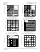
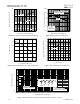
MOSFET symbol
V
GS
= 20V
V
GS
= -20V
V
DS
= 25V, I
D
= 7.7A
and center of die contact
I
D
= 7.7A
R
G
= 2.5Ω
V
DS
= V
GS
, I
D
= 25µA
V
DS
= 55V, V
GS
= 0V
V
DS
= 55V, V
GS
= 0V, T
J
= 125°C
Conditions
V
GS
= 0V, I
D
= 250µA
Reference to 25°C, I
D
= 1mA
V
GS
= 10V, I
D
= 7.7A
e
V
DS
= 44V
V
GS
= 0V
V
DS
= 50V
ƒ = 1.0MHz, See Fig. 5
V
GS
= 10V
I
D
= 7.7A
V
DD
= 28V, V
GS
= 10V
e