
Datasheet

IRFHS8342PbF
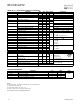
www.irf.com 5
Fig 13. Typical On-Resistance vs. Drain Current
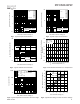
Fig 12. On-Resistance vs. Gate Voltage
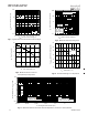
Fig 14. Typical Power vs. Time
Fig 15. Peak Diode Recovery dv/dt Test Circuit for N-Channel
HEXFET
®
Power MOSFETs
Circuit Layout Considerations
• Low Stray Inductance
• Ground Plane
• Low Leakage Inductance
Current Transformer
P.W.
Period
di/dt
Diode Recovery
dv/dt
Ripple ≤ 5%
Body Diode Forward Drop
Re-Applied
Voltage
Reverse
Recovery
Current
Body Diode Forward
Current
V
GS
=10V
V
DD
I
SD
Driver Gate Drive
D.U.T. I
SD
Waveform
D.U.T. V
DS
Waveform
Inductor Curent
D =
P. W .
Period
* V
GS
= 5V for Logic Level Devices
*
+
-
+
+
+
-
-
-
R
G
V
DD
• dv/dt controlled by R
G
• Driver same type as D.U.T.
• I
SD
controlled by Duty Factor "D"
• D.U.T. - Device Under Test
D.U.T
1E-5 1E-4 1E-3 1E-2 1E-1 1E+0
Time (sec)
0
100
200
300
400
500
600
S
i
n
g
l
e
P
u
l
s
e
P
o
w
e
r
(
W
)
0 5 10 15 20
V
GS,
Gate -to -Source Voltage (V)
5
10
15
20
25
30
35
R
D
S
(
o
n
)
,
D
r
a
i
n
-
t
o
-
S
o
u
r
c
e
O
n
R
e
s
i
s
t
a
n
c
e
(
m
Ω
)
I
D
= 8.5A
T
J
= 125°C
T
J
= 25°C
0 10 20 30 40 50 60 70
I
D
, Drain Current (A)
5
10
15
20
25
30
R
D
S
(
o
n
)
,
D
r
a
i
n
-
t
o
-
S
o
u
r
c
e
O
n
R
e
s
i
s
t
a
n
c
e
(
m
Ω
)
Vgs = 4.5V
Vgs = 10V