
Datasheet

IRFHS8342PbF
2 www.irf.com
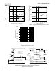
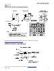
D
S
G
Notes:
Repetitive rating; pulse width limited by max. junction temperature.
Current limited by package.
Pulse width ≤ 400μs; duty cycle ≤ 2%.
When mounted on 1 inch square copper board
R
θ
is measured at T
J
of approximately 90°C.
Th
erma
l R
es
i
s
t
ance
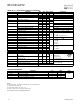
Parameter Typ. Max. Units
R
θ
JC
(Bottom)
Junction-to-Case
––– 13
R
θJC
(Top)
Junction-to-Case
––– 90
°C/W
R
θ
JA
Junction-to-Ambient
––– 60
R
θ
JA
Junction-to-Ambient (<10s)
––– 42
Static @ T
J
= 25°C (unless otherwise specified)
Parameter Min. Typ. Max. Units
BV
DSS
Drain-to-Source Breakdown Voltage 30 ––– ––– V
ΔΒV
DSS
/ΔT
J
Breakdown Voltage Temp. Coefficient ––– 22 ––– mV/°C
R
DS(on)
Static Drain-to-Source On-Resistance ––– 13 16
––– 20 25
V
GS(th)
Gate Threshold Voltage 1.35 1.8 2.35 V
ΔV
GS(th)
Gate Threshold Voltage Coefficient ––– -5.8 ––– mV/°C
I
DSS
Drain-to-Source Leakage Current ––– ––– 1.0
––– ––– 150
I
GSS
Gate-to-Source Forward Leakage ––– ––– 100
Gate-to-Source Reverse Leakage ––– ––– -100
gfs Forward Transconductance 18 ––– ––– S
Q
g
Total Gate Charge ––– 4.2 ––– nC
Q
g
Total Gate Charge ––– 8.7 –––
V
DS
= 15V
Q
gs
Gate-to-Source Charge ––– 1.5 –––
Q
gd
Gate-to-Drain Charge ––– 1.3 –––
R
G
Gate Resistance ––– 1.9
–––
Ω
t
d(on)
Turn-On Delay Time ––– 5.9 –––
t
r
Rise Time –––15–––
t
d(off)
Turn-Off Delay Time ––– 5.2 –––
t
f
Fall Time ––– 5.0 –––
C
iss
Input Capacitance ––– 600 –––
C
oss
Output Capacitance ––– 100 –––
C
rss
Reverse Transfer Capacitance ––– 46 –––
Diode Characteristics
Parameter Min. Typ. Max. Units
I
S
Continuous Source Current
(Body Diode)
I
SM
Pulsed Source Current
(
Bod
y
Diode
)
V
SD
Diode Forward Voltage ––– ––– 1.0 V
t
rr
Reverse Recovery Time ––– 11 17 ns
Q
rr
Reverse Recovery Charge ––– 13 20 nC
t
on
Forward Turn-On Time Time is dominated by parasitic Inductance
V
DS
= V
GS
, I
D
= 25μA
V
GS
= 4.5V, I
D
= 6.8A
mΩ
V
DD
= 15V, V
GS
= 4.5V
V
GS
= 4.5V, V
DS
= 15V, I
D
= 8.5A
R
G
=1.8Ω
V
DS
= 10V, I
D
= 8.5A
V
DS
= 24V, V
GS
= 0V, T
J
= 125°C
μA
I
D
= 8.5A (See Fig. 6 & 16)
I
D
= 8.5A
V
GS
= 0V
V
DS
= 25V
V
DS
= 24V, V
GS
= 0V
T
J
= 25°C, I
F
= 8.5A , V
DD
= 13V
di/dt = 330 A/μs
T
J
= 25°C, I
S
= 8.5A , V
GS
= 0V
showing the
integral reverse
p-n junction diode.
Conditions
See Fig.17
ƒ = 1.0MHz
Conditions
V
GS
= 0V, I
D
= 250μA
Reference to 25°C, I
D
= 1mA
V
GS
= 10V, I
D
= 8.5A
––– ––– 76
––– ––– 8.5
MOSFET symbol
nA
ns
A
pF
nC
V
GS
= 10V
V
GS
= 20V
V
GS
= -20V