
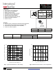
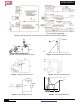
Datasheet


2 www.irf.com © 2014 International Rectifier Submit Datasheet Feedback November 7, 2014
IRFB7546PbF
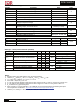
Absolute Maximum Rating
Symbol Parameter Max. Units
I
D
@ T
C
= 25°C Continuous Drain Current, V
GS
@ 10V 75
A
I
D
@ T
C
= 100°C Continuous Drain Current, V
GS
@ 10V 53
I
DM
Pulsed Drain Current 300
P
D
@T
C
= 25°C Maximum Power Dissipation 99 W
Linear Derating Factor 0.7 W/°C
V
GS
Gate-to-Source Voltage ± 20 V
T
J
T
STG
Operating Junction and
Storage Temperature Range
-55 to + 175
°C
Soldering Temperature, for 10 seconds (1.6mm from case) 300
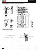
Mounting Torque, 6-32 or M3 Screw 10 lbf·in (1.1 N·m)
Avalanche Characteristics
E
AS (Thermally limited)
Single Pulse Avalanche Energy
110
mJ
E
AS (Thermally limited)
Single Pulse Avalanche Energy
170
I
AR
Avalanche Current
See Fig 15, 16, 23a, 23b
A
E
AR
Repetitive Avalanche Energy mJ
Thermal Resistance
Symbol Parameter Typ. Max. Units
R
JC
Junction-to-Case
––– 1.52
R
CS
Case-to-Sink, Flat Greased Surface
0.50 –––
R
JA
Junction-to-Ambient
––– 62
°C/W
Static @ T
J
= 25°C (unless otherwise specified)
Symbol Parameter Min. Typ. Max. Units Conditions
V
(BR)DSS
Drain-to-Source Breakdown Voltage 60 ––– ––– V V
GS
= 0V, I
D
= 250µA
V
(BR)DSS
/T
J
Breakdown Voltage Temp. Coefficient ––– 46 ––– mV/°C Reference to 25°C, I
D
= 1mA
R
DS(on)
––– 6.0 7.3
m
V
GS
= 10V, I
D
= 45A
––– 7.5 ––– V
GS
= 6.0V, I
D
= 23A
V
GS(th)
Gate Threshold Voltage 2.1 ––– 3.7 V V
DS
= V
GS
, I
D
= 100µA
I
DSS
Drain-to-Source Leakage Current
––– ––– 1.0
µA
V
DS
=60 V, V
GS
= 0V
––– ––– 150 V
DS
=60V,V
GS
= 0V,T
J
=125°C
I
GSS
Gate-to-Source Forward Leakage ––– ––– 100
nA
V
GS
= 20V
Gate-to-Source Reverse Leakage ––– ––– -100 V
GS
= -20V
R
G
Gate Resistance ––– 1.6 –––
Static Drain-to-Source On-Resistance
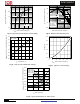
Notes:
Repetitive rating; pulse width limited by max. junction temperature.
Limited by T
Jmax
, starting T
J
= 25°C, L = 110µH, R
G
= 50, I
AS
= 45A, V
GS
=10V.
I
SD
100A, di/dt 1260A/µs, V
DD
V
(BR)DSS
, T
J
175°C.
Pulse width 400µs; duty cycle 2%.
C
oss
eff. (TR) is a fixed capacitance that gives the same charging time as C
oss
while V
DS
is rising from 0 to 80% V
DSS
.
C
oss
eff. (ER) is a fixed capacitance that gives the same energy as C
oss
while V
DS
is rising from 0 to 80% V
DSS
.
R
is measured at T
J
approximately 90°C.
When mounted on 1" square PCB (FR-4 or G-10 Material). For recommended footprint and soldering techniques
refer to application note #AN-994.: http://www.irf.com/technical-info/appnotes/an-994.pdf
Limited by T
Jmax
, starting T
J
= 25°C, L = 1mH, R
G
= 50, I
AS
= 19A, V
GS
=10V