
Datasheet

3 www.irf.com © 2014 International Rectifier Submit Datasheet Feedback October 7, 2014
IRFB/S/SL7537PbF
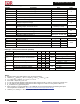
Dynamic Electrical Characteristics @ T
J
= 25°C (unless otherwise specified)
Symbol Parameter Min. Typ. Max. Units Conditions
gfs Forward Transconductance 190 ––– ––– S V
DS
= 10V, I
D
=100A
Q
g
Total Gate Charge ––– 142 210
I
D
= 100A
Q
gs
Gate-to-Source Charge ––– 36 ––– V
DS
= 30V
Q
gd
Gate-to-Drain Charge ––– 43 ––– V
GS
= 10V
Q
sync
Total Gate Charge Sync. (Qg– Qgd) ––– 99 –––
t
d(on)
Turn-On Delay Time ––– 15 –––
ns
V
DD
= 30V
t
r
Rise Time ––– 105 ––– I
D
= 100A
t
d(off)
Turn-Off Delay Time ––– 82 –––
R
G
= 2.7
t
f
Fall Time ––– 84 –––
V
GS
= 10V
C
iss
Input Capacitance ––– 7020 –––
pF
V
GS
= 0V
C
oss
Output Capacitance ––– 640 ––– V
DS
= 25V
C
rss
Reverse Transfer Capacitance ––– 395 –––
ƒ = 1.0MHz, See Fig.7
C
oss eff.(ER)
Effective Output Capacitance
(Energy Related)
––– 665 ––– V
GS
= 0V, VDS = 0V to 48V
C
oss eff.(TR)
Output Capacitance (Time Related) ––– 880 ––– V
GS
= 0V, VDS = 0V to 48V
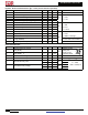
Diode Characteristics
Symbol Parameter Min. Typ. Max. Units Conditions
I
S
Continuous Source Current
––– ––– 173
A
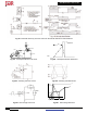
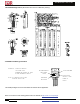
MOSFET symbol
(Body Diode)
showing the
I
SM
Pulsed Source Current
––– ––– 700
integral reverse
(Body Diode) p-n junction diode.
V
SD
Diode Forward Voltage ––– ––– 1.2 V T
J
= 25°C,I
S
= 100A,V
GS
= 0V
dv/dt Peak Diode Recovery dv/dt ––– 10 ––– V/ns T
J
= 175°C,I
S
=100A,V
DS
= 60V
t
rr
Reverse Recovery Time
––– 39 –––
ns
T
J
= 25°C V
DD
= 51V
––– 41 ––– T
J
= 125°C I
F
= 100A,
Q
rr
Reverse Recovery Charge
––– 46 –––
nC
T
J
= 25°C di/dt = 100A/µs
––– 56 ––– T
J
= 125°C
I
RRM
Reverse Recovery Current ––– 2.1 ––– A
T
J
= 25°C
nC
D
S
G