
Datasheet


2 www.irf.com © 2014 International Rectifier Submit Datasheet Feedback November 7, 2014
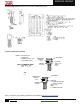
IRFB/S/SL7530PbF
Absolute Maximum Rating
Symbol Parameter Max. Units
I
D
@ T
C
= 25°C Continuous Drain Current, V
GS
@ 10V (Silicon Limited) 295
A
I
D
@ T
C
= 100°C Continuous Drain Current, V
GS
@ 10V (Silicon Limited) 208
I
D
@ T
C
= 25°C Continuous Drain Current, V
GS
@ 10V (Wire Bond Limited) 195
I
DM
Pulsed Drain Current 760
P
D
@T
C
= 25°C Maximum Power Dissipation 375 W
Linear Derating Factor 2.5 W/°C
V
GS
Gate-to-Source Voltage ± 20 V
T
J
T
STG
Operating Junction and
Storage Temperature Range
-55 to + 175
°C
Soldering Temperature, for 10 seconds (1.6mm from case) 300
Mounting Torque, 6-32 or M3 Screw 10 lbf·in (1.1 N·m)
Avalanche Characteristics
E
AS (Thermally limited)
Single Pulse Avalanche Energy
524
mJ
E
AS (Thermally limited)
Single Pulse Avalanche Energy
1025
I
AR
Avalanche Current
See Fig 15, 16, 23a, 23b
A
E
AR
Repetitive Avalanche Energy mJ
Thermal Resistance
Symbol Parameter Typ. Max. Units
R
JC
Junction-to-Case
––– 0.40
°C/W
R
CS
Case-to-Sink, Flat Greased Surface
0.50 –––
R
JA
Junction-to-Ambient (PCB Mount) (D
2
-Pak)
––– 40
R
JA
Junction-to-Ambient (TO-220)
––– 62
Static @ T
J
= 25°C (unless otherwise specified)
Symbol Parameter Min. Typ. Max. Units Conditions
V
(BR)DSS
Drain-to-Source Breakdown Voltage 60 ––– ––– V V
GS
= 0V, I
D
= 250µA
V
(BR)DSS
/T
J
Breakdown Voltage Temp. Coefficient ––– 47 ––– mV/°C Reference to 25°C, I
D
= 1mA
R
DS(on)
Static Drain-to-Source On-Resistance
––– 1.65 2.00
m
V
GS
= 10V, I
D
= 100A
V
GS(th)
Gate Threshold Voltage 2.1 ––– 3.7 V V
DS
= V
GS
, I
D
= 250µA
I
DSS
Drain-to-Source Leakage Current
––– ––– 1.0
µA
V
DS
=60 V, V
GS
= 0V
––– ––– 150 V
DS
=60V,V
GS
= 0V,T
J
=125°C
I
GSS
Gate-to-Source Forward Leakage ––– ––– 100
nA
V
GS
= 20V
Gate-to-Source Reverse Leakage ––– ––– -100 V
GS
= -20V
R
G
Gate Resistance ––– 2.1 –––
––– 2.10 –––
V
GS
= 6.0V, I
D
= 50A
Notes:
Calculated continuous current based on maximum allowable junction temperature. Bond wire current limit is 195A by
source bonding technology. Note that current limitations arising from heating of the device leads may occur with
some lead mounting arrangements. (Refer to AN-1140)
Repetitive rating; pulse width limited by max. junction temperature.
Limited by T
Jmax
, starting T
J
= 25°C, L = 105µH, R
G
= 50, I
AS
= 100A, V
GS
=10V.
I
SD
100A, di/dt 1338A/µs, V
DD
V
(BR)DSS
, T
J
175°C.
Pulse width 400µs; duty cycle 2%.
C
oss
eff. (TR) is a fixed capacitance that gives the same charging time as C
oss
while V
DS
is rising from 0 to 80% V
DSS
.
C
oss
eff. (ER) is a fixed capacitance that gives the same energy as C
oss
while V
DS
is rising from 0 to 80% V
DSS
.
R
is measured at T
J
approximately 90°C.
When mounted on 1" square PCB (FR-4 or G-10 Material). For recommended footprint and soldering techniques refer to
application note #AN-994.: http://www.irf.com/technical-info/appnotes/an-994.pdf
Limited by T
Jmax
, starting T
J
= 25°C, L = 1mH, R
G
= 50, I
AS
= 45A, V
GS
=10V.