
Datasheet


IRFB4332PbF
2 www.irf.com
S
D
G
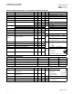
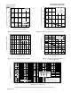
Electrical Characteristics @ T
J
= 25°C (unless otherwise specified)
Parameter Min. Typ. Max. Units
BV
DSS
Drain-to-Source Breakdown Voltage 250 ––– ––– V
ΔΒV
DSS
/ΔT
J
Breakdown Voltage Temp. Coefficient ––– 170 ––– mV/°C
R
DS(on)
Static Drain-to-Source On-Resistance ––– 29 33
mΩ
V
GS(th)
Gate Threshold Voltage 3.0 ––– 5.0 V
ΔV
GS(th)
/ΔT
J
Gate Threshold Voltage Coefficient ––– -14 ––– mV/°C
I
DSS
Drain-to-Source Leakage Current ––– ––– 20 μA
––– ––– 1.0 mA
I
GSS
Gate-to-Source Forward Leakage ––– ––– 100 nA
Gate-to-Source Reverse Leakage ––– ––– -100
g
fs
Forward Transconductance 100 ––– ––– S
Q
g
Total Gate Charge ––– 99 150 nC
Q
gd
Gate-to-Drain Charge ––– 35 –––
t
st
Shoot Through Blocking Time 100 ––– ––– ns
E
PULSE
Energy per Pulse μJ
C
iss
Input Capacitance ––– 5860 –––
C
oss
Output Capacitance ––– 530 ––– pF
C
rss
Reverse Transfer Capacitance ––– 130 –––
C
oss
eff.
Effective Output Capacitance ––– 360 –––
L
D
Internal Drain Inductance ––– 4.5 ––– Between lead,
nH 6mm (0.25in.)
L
S
Internal Source Inductance ––– 7.5 ––– from package
Avalanche Characteristics
Parameter Units
E
AS
Single Pulse Avalanche Energy
d
mJ
E
AR
Repetitive Avalanche Energy
c
mJ
V
DS(Avalanche)
Repetitive Avalanche Voltage
c
V
I
AS
Avalanche Current
d
A
Diode Characteristics
Parameter Min. Typ. Max. Units
I
S
@ T
C
= 25°C
Continuous Source Current ––– ––– 60
(Body Diode) A
I
SM
Pulsed Source Current ––– ––– 230
(Body Diode)
c
V
SD
Diode Forward Voltage ––– ––– 1.3 V
t
rr
Reverse Recovery Time ––– 190 290 ns
Q
rr
Reverse Recovery Charge ––– 820 1230 nC
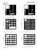
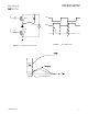
MOSFET symbol
V
DS
= 25V, I
D
= 35A
V
DD
= 125V, I
D
= 35A, V
GS
= 10V
e
Conditions
and center of die contact
V
DD
= 200V, V
GS
= 15V, R
G
= 4.7Ω
V
DS
= 200V, R
G
= 5.1Ω, T
J
= 25°C
L = 220nH, C= 0.3μF, V
GS
= 15V
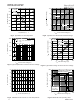
V
DS
= 200V, R
G
= 5.1Ω, T
J
= 100°C
V
DS
= 25V
V
DS
= V
GS
, I
D
= 250μA
V
DS
= 250V, V
GS
= 0V
V
GS
= 0V, V
DS
= 0V to 200V
V
DS
= 250V, V
GS
= 0V, T
J
= 125°C
V
GS
= 20V
V
GS
= -20V
V
GS
= 0V
L = 220nH, C= 0.3μF, V
GS
= 15V
Conditions
V
GS
= 0V, I
D
= 250μA
Reference to 25°C, I
D
= 1mA
V
GS
= 10V, I
D
= 35A
e
T
J
= 25°C, I
F
= 35A, V
DD
= 50V
di/dt = 100A/μs
e
T
J
= 25°C, I
S
= 35A, V
GS
= 0V
e
showing the
integral reverse
p-n junction diode.
Typ. Max.
ƒ = 1.0MHz,
––– 230
39
35
–––
–––
300 –––
––– 520 –––
––– 920 –––