
Datasheet

IRF/B/S/SL4310PbF
2 www.irf.com
Notes:
Calculated continuous current based on maximum allowable junction
temperature. Package limitation current is 75A
Repetitive rating; pulse width limited by max. junction
temperature.
Limited by T
Jmax
, starting T
J
= 25°C, L = 0.35mH
R
G
= 25Ω, I
AS
= 75A, V
GS
=10V. Part not recommended for use
above this value.
I
SD
≤ 75A, di/dt ≤ 550A/µs, V
DD
≤ V
(BR)DSS
, T
J
≤ 175°C.
Pulse width ≤ 400µs; duty cycle ≤ 2%.
S
D
G
C
oss
eff. (TR) is a fixed capacitance that gives the same charging time
as C
oss
while V
DS
is rising from 0 to 80% V
DSS
.
C
oss
eff. (ER) is a fixed capacitance that gives the same energy as
C
oss
while V
DS
is rising from 0 to 80% V
DSS
.
When mounted on 1" square PCB (FR-4 or G-10 Material). For recommended
footprint and soldering techniques refer to application note #AN-994.
R
θ
is measured at T
J
approximately 90°C.
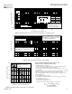
Static @ T
J
= 25°C (unless otherwise specified)
Symbol Parameter Min. Typ. Max. Units
V
(BR)DSS
Drain-to-Source Breakdown Voltage 100 ––– ––– V
∆
V
(BR)DSS
/
∆
T
J
Breakdown Voltage Temp. Coefficient ––– 0.064 ––– V/°C
R
DS(on)
Static Drain-to-Source On-Resistance ––– 5.6 7.0
mΩ
V
GS(th)
Gate Threshold Voltage 2.0 ––– 4.0 V
I
DSS
Drain-to-Source Leakage Current ––– ––– 20 µA
––– ––– 250
I
GSS
Gate-to-Source Forward Leakage ––– ––– 200 nA
Gate-to-Source Reverse Leakage ––– ––– -200
R
G
Gate Input Resistance ––– 1.4 –––
Ω
f = 1MHz, open drain
Dynamic @ T
J
= 25°C (unless otherwise specified)
Symbol Parameter Min. Typ. Max. Units
gfs Forward Transconductance 160 ––– ––– S
Q
g
Total Gate Charge ––– 170 250 nC
Q
gs
Gate-to-Source Charge ––– 46 –––
Q
gd
Gate-to-Drain ("Miller") Charge ––– 62 –––
t
d(on)
Turn-On Delay Time ––– 26 ––– ns
t
r
Rise Time ––– 110 –––
t
d(off)
Turn-Off Delay Time ––– 68 –––
t
f
Fall Time ––– 78 –––
C
iss
Input Capacitance ––– 7670 ––– pF
C
oss
Output Capacitance ––– 540 –––
C
rss
Reverse Transfer Capacitance ––– 280 –––
C
oss
eff. (ER)
Effective Output Capacitance (Energy Related)
––– 650 –––
C
oss
eff. (TR)
Effective Output Capacitance (Time Related)
––– 720.1 –––
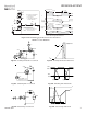
Diode Characteristics
Symbol Parameter Min. Typ. Max. Units
I
S
Continuous Source Current ––– –––
130
A
(Body Diode)
I
SM
Pulsed Source Current ––– ––– 550
(Body Diode)
V
SD
Diode Forward Voltage ––– ––– 1.3 V
t
rr
Reverse Recovery Time ––– 45 68 ns
T
J
= 25°C
V
R
= 85V,
––– 55 83
T
J
= 125°C
I
F
= 75A
Q
rr
Reverse Recovery Charge ––– 82 120 nC
T
J
= 25°C
di/dt = 100A/µs
––– 120 180
T
J
= 125°C
I
RRM
Reverse Recovery Current ––– 3.3 ––– A
T
J
= 25°C
t
on
Forward Turn-On Time Intrinsic turn-on time is negligible (turn-on is dominated by LS+LD)
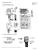
Conditions
V
DS
= 50V, I
D
= 75A
I
D
= 75A
V
GS
= 20V
V
GS
= -20V
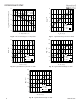
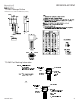
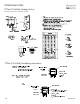
MOSFET symbol
showing the
V
DS
= 80V
Conditions
V
GS
= 10V
V
GS
= 0V
V
DS
= 50V
ƒ = 1.0MHz
V
GS
= 0V, V
DS
= 0V to 80V , See Fig.11
V
GS
= 0V, V
DS
= 0V to 80V , See Fig. 5
T
J
= 25°C, I
S
= 75A, V
GS
= 0V
integral reverse
p-n junction diode.
Conditions
V
GS
= 0V, I
D
= 250µA
Reference to 25°C, I
D
= 1mA
V
GS
= 10V, I
D
= 75A
V
DS
= V
GS
, I
D
= 250µA
V
DS
= 100V, V
GS
= 0V
V
DS
= 100V, V
GS
= 0V, T
J
= 125°C
I
D
= 75A
R
G
= 2.6
Ω
V
GS
= 10V
V
DD
= 65V