
Datasheet


IRFB4229PbF
6 www.irf.com
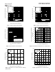
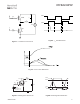
Fig 19b. Unclamped Inductive Waveforms
Fig 19a. Unclamped Inductive Test Circuit
t
p
V
(BR)DSS
I
AS
R
G
I
AS
0.01
Ω
t
p
D.U.T
L
V
DS
+
-
V
DD
DRIVER
A
15V
20V
V
GS
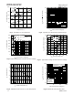
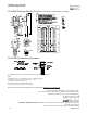
Fig 20a. Gate Charge Test Circuit
Fig 20b. Gate Charge Waveform
Vds
Vgs
Id
Vgs(th)
Qgs1
Qgs2 Qgd Qgodr
Fig 18. Diode Reverse Recovery Test Circuit for HEXFET
®
Power MOSFETs
Circuit Layout Considerations
• Low Stray Inductance
• Ground Plane
• Low Leakage Inductance
Current Transformer
P.W.
Period
di/dt
Diode Recovery
dv/dt
Ripple ≤ 5%
Body Diode Forward Drop
Re-Applied
Voltage
Reverse
Recovery
Current
Body Diode Forward
Current
V
GS
=10V
V
DD
I
SD
Driver Gate Drive
D.U.T. I
SD
Waveform
D.U.T. V
DS
Waveform
Inductor Curent
D =
P. W .
Period
*** V
GS
= 5V for Logic Level Devices
***
+
-
+
+
+
-
-
-
R
G
V
DD
• dv/dt controlled by R
G
• Driver same type as D.U.T.
• I
SD
controlled by Duty Factor "D"
• D.U.T. - Device Under Test
D.U.T
**
*
*
Use P-Channel Driver for P-Channel Measurements
** Reverse Polarity for P-Channel
1K
VCC
DUT
0
L