
Datasheet
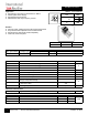

IRFB4137PbF
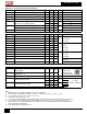
6
www.irf.com © 2012 International Rectifier October 30, 2012
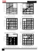
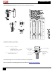
Fig 18. Peak Diode Recovery dv/dt Test Circuit for N-Channel HEXFET
®
Power MOSFETs
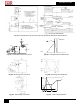
Fig 19a. Unclamped Inductive Test Circuit
R
G
I
AS
0.01
t
p
D.U.T
L
V
DS
+
-
V
DD
DRIVER
A
15V
20V
Fig 20a. Switching Time Test Circuit
Fig 21a. Gate Charge Test Circuit
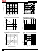
t
p
V
(BR)DSS
I
AS
Fig 19b. Unclamped Inductive Waveforms
Fig 20b. Switching Time Waveforms
Vds
Vgs
Id
Vgs(th)
Qgs1
Qgs2 Qgd Qgodr
Fig 21b. Gate Charge Waveform