
Datasheet

IRFB4110PbF
2 www.irf.com
Notes:
Calculated continuous current based on maximum allowable junction
temperature. Bond wire current limit is 120A. Note that current
limitations arising from heating of the device leads may occur with
some lead mounting arrangements.
Repetitive rating; pulse width limited by max. junction
temperature.
Limited by T
Jmax
, starting T
J
= 25°C, L = 0.033mH
R
G
= 25Ω, I
AS
= 108A, V
GS
=10V. Part not recommended for use
above this value.
S
D
G
I
SD
≤ 75A, di/dt ≤ 630A/μs, V
DD
≤ V
(BR)DSS
, T
J
≤ 175°C.
Pulse width ≤ 400μs; duty cycle ≤ 2%.
C
oss
eff. (TR) is a fixed capacitance that gives the same charging time
as C
oss
while V
DS
is rising from 0 to 80% V
DSS
.
C
oss
eff. (ER) is a fixed capacitance that gives the same energy as
C
oss
while V
DS
is rising from 0 to 80% V
DSS
.
When mounted on 1" square PCB (FR-4 or G-10 Material). For recom
mended footprint and soldering techniques refer to application note #AN-994.
R
θ
is measured at T
J
approximately 90°C.
Static @ T
J
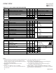
= 25°C (unless otherwise specified)
Symbol
Parameter
Min.
Typ.
Max.
Units
V
(BR)DSS
Drain-to-Source Breakdown Voltage
100
–––
–––
V
Δ
V
(BR)DSS
/
Δ
T
J
Breakdown Voltage Temp. Coefficient
–––
0.108
–––
V/°C
R
DS(on)
Static Drain-to-Source On-Resistance
–––
3.7
4.5
m
Ω
V
GS(th)
Gate Threshold Voltage
2.0
–––
4.0
V
I
DSS
Drain-to-Source Leakage Current
–––
–––
20
μA
–––
–––
250
I
GSS
Gate-to-Source Forward Leakage
–––
–––
100
nA
Gate-to-Source Reverse Leakage
–––
–––
-100
Dynamic @ T
J
= 25°C (unless otherwise specified)
Symbol
Parameter
Min.
Typ.
Max.
Units
gfs
Forward Transconductance
160
–––
–––
S
Q
g
Total Gate Charge
–––
150
210
nC
Q
gs
Gate-to-Source Charge
–––
35
–––
Q
gd
Gate-to-Drain ("Miller") Charge
–––
43
–––
R
G
Gate Resistance
–––
1.3 ––– Ω
t
d(on)
Turn-On Delay Time
–––
25
–––
ns
t
r
Rise Time
–––
67
–––
t
d(off)
Turn-Off Delay Time
–––
78
–––
t
f
Fall Time
–––
88
–––
C
iss
Input Capacitance
–––
9620
–––
pF
C
oss
Output Capacitance
–––
670
–––
C
rss
Reverse Transfer Capacitance
–––
250
–––
C
oss
eff. (ER)
Effective Output Capacitance (Energy Related)
–––
820
–––
C
oss
eff. (TR)
Effective Output Capacitance (Time Related)
–––
950
–––
Diode Characteristics
Symbol
Parameter
Min.
Typ.
Max.
Units
I
S
Continuous Source Current
–––
–––
170
A
(Body Diode)
I
SM
Pulsed Source Current
–––
–––
670
(Body Diode)
V
SD
Diode Forward Voltage
–––
–––
1.3
V
t
rr
Reverse Recovery Time
–––
50
75
ns
T
J
= 25°C
V
R
= 85V,
–––
60
90
T
J
= 125°C
I
F
= 75A
Q
rr
Reverse Recovery Charge
–––
94
140
nC
T
J
= 25°C
di/dt = 100A/μs
–––
140
210
T
J
= 125°C
I
RRM
Reverse Recovery Current
–––
3.5
–––
A
T
J
= 25°C
t
on
Forward Turn-On Time
Intrinsic turn-on time is negligible (turn-on is dominated by LS+LD)
I
D
= 75A
R
G
= 2.6
Ω
V
GS
= 10V
V
DD
= 65V
T
J
= 25°C, I
S
= 75A, V
GS
= 0V
integral reverse
p-n junction diode.
Conditions
V
GS
= 0V, I
D
= 250μA
Reference to 25°C, I
D
= 5mA
V
GS
= 10V, I
D
= 75A
V
DS
= V
GS
, I
D
= 250μA
V
DS
= 100V, V
GS
= 0V
V
DS
= 100V, V
GS
= 0V, T
J
= 125°C
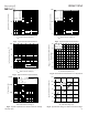
MOSFET symbol
showing the
V
DS
= 50V
Conditions
V
GS
= 10V
V
GS
= 0V
V
DS
= 50V
ƒ = 1.0MHz
V
GS
= 0V, V
DS
= 0V to 80V
V
GS
= 0V, V
DS
= 0V to 80V
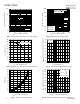
Conditions
V
DS
= 50V, I
D
= 75A
I
D
= 75A
V
GS
= 20V
V
GS
= -20V