
Datasheet


IRF8721PbF
6 www.irf.com
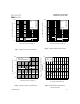
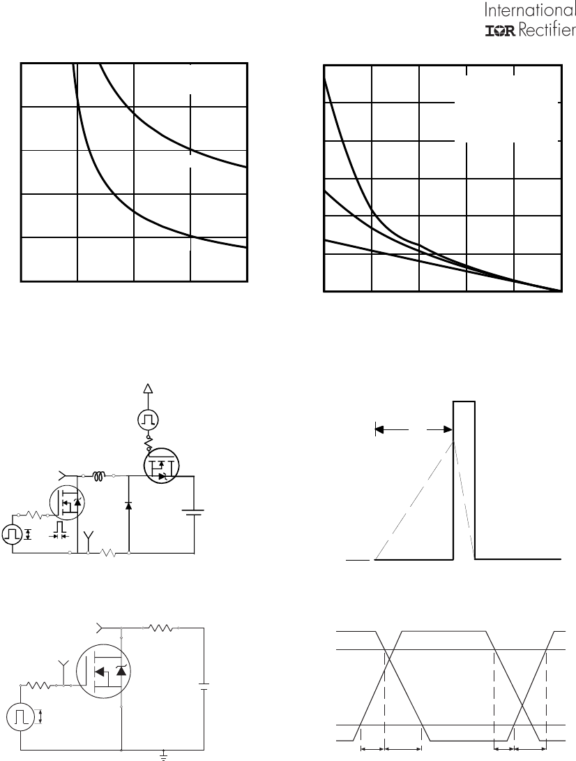
Fig 13. Maximum Avalanche Energy
vs. Drain Current
Fig 12. On-Resistance vs. Gate Voltage
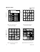
Fig 15b. Switching Time Waveforms
Fig 14b. Unclamped Inductive Waveforms
Fig 14a. Unclamped Inductive Test Circuit
t
p
V
(BR)DSS
I
AS
Fig 15a. Switching Time Test Circuit
2.0 4.0 6.0 8.0 10.0
V
GS
, Gate-to-Source Voltage (V)
6
8
10
12
14
16
R
D
S
(
o
n
)
,
D
r
a
i
n
-
t
o
-
S
o
u
r
c
e
O
n
R
e
s
i
s
t
a
n
c
e
(
m
Ω
)
T
J
= 25°C
T
J
= 125°C
I
D
= 14A
R
G
I
AS
0.01
Ω
t
p
D.U.T
L
V
DS
+
-
V
DD
DRIVER
A
15V
20V
25 50 75 100 125 150
Starting T
J
, Junction Temperature (°C)
0
50
100
150
200
250
300
E
A
S
,
S
i
n
g
l
e
P
u
l
s
e
A
v
a
l
a
n
c
h
e
E
n
e
r
g
y
(
m
J
)
I
D
TOP
0.83A
1.05A
BOTTOM
11A
V
DS
90%
10%
V
GS
t
d(on)
t
r
t
d(off)
t
f
V
DS
Pulse Width ≤ 1 µs
Duty Factor ≤ 0.1
R
D
V
GS
R
G
D.U.T.
10V
+
-
V
DD
V
GS