
Datasheet

IRF7459
www.irf.com 5
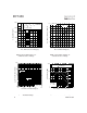
Fig 11. Maximum Effective Transient Thermal Impedance, Junction-to-Ambient
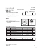
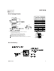
Fig 9. Maximum Drain Current Vs.
Case Temperature
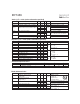
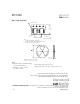
Fig 10a. Switching Time Test Circuit
V
DS
90%
10%
V
GS
t
d(on)
t
r
t
d(off)
t
f
Fig 10b. Switching Time Waveforms
V
DS
Pulse Width ≤ 1 µs
Duty Factor ≤ 0.1 %
R
D
V
GS
R
G
D.U.T.
10V
+
-
V
DD
0.01
0.1
1
10
100
0.00001 0.0001 0.001 0.01 0.1 1 10 100
Notes:
1. Duty factor D = t / t
2. Peak T =P x Z + T
1 2
J DM thJA A
P
t
t
DM
1
2
t , Rectan
g
ular Pulse Duration
(
sec
)
Thermal Response (Z )
1
thJA
0.01
0.02
0.05
0.10
0.20
D = 0.50
SINGLE PULSE
(THERMAL RESPONSE)
25 50 75 100 125 150
0
3
6
9
12
15
T , Case Temperature ( C)
I , Drain Current (A)
°
C
D