
Datasheet


IRF7457PbF
6 www.irf.com
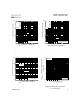
Fig 14. On-Resistance Vs. Gate Voltage
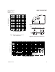
Fig 12. On-Resistance Vs. Drain Current
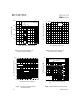
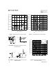
Fig 13a&b. Basic Gate Charge Test Circuit
and Waveform
Fig 14a&b. Unclamped Inductive Test circuit
and Waveforms
Fig 14c. Maximum Avalanche Energy
Vs. Drain Current
D.U.T.
V
DS
I
D
I
G
3mA
V
GS
.3µF
50KΩ
.2µF
12V
Current Regulator
Same Type as D.U.T.
Current Sampling Resistors
+
-
V
GS
Q
G
Q
GS
Q
GD
V
G
Charge
t
p
V
(BR)DSS
I
AS
R
G
I
AS
0.01
Ω
t
p
D.U.T
L
V
DS
+
-
V
DD
DRIVER
A
15V
20V
0 20 40 60 80 100 120
I
D
, Drain Current ( A )
0.000
0.005
0.010
0.015
0.020
0.025
0.030
R
D
S
(
o
n
)
,
D
r
a
i
n
-
t
o
-
S
o
u
r
c
e
O
n
R
e
s
i
s
t
a
n
c
e
(
Ω
)
VGS = 4.5V
VGS = 10V
3.0 3.5 4.0 4.5 5.0 5.5
V
GS,
Gate -to -Source Voltage (V)
0.006
0.008
0.010
0.012
0.014
0.016
0.018
0.020
R
D
S
(
o
n
)
,
D
r
a
i
n
-
t
o
-
S
o
u
r
c
e
O
n
R
e
s
i
s
t
a
n
c
e
(
Ω
)
I
D
= 15A
25 50 75 100 125 150
0
100
200
300
400
500
600
700
Starting T , Junction Temperature ( C)
E , Single Pulse Avalanche Energy (mJ)
J
AS
°
I
D
TOP
BOTTOM
5.4A
9.6A
12A