
Datasheet

IRF7421D1
www.irf.com 5
Power Mosfet Characteristics
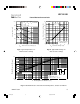
Fig 10. Typical Gate Charge Vs.
Gate-to-Source Voltage
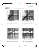
Fig 9. Typical Capacitance Vs.
Drain-to-Source Voltage
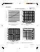
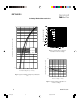
Fig 9. Maximum Effective Transient Thermal Impedance, Junction-to-Ambient
0
200
400
600
800
1000
1 10 100
C, Capacitance (pF)
DS
V , Drain-to-Source Voltage (V)
A
V = 0V, f = 1MHz
C = C + C , C SHORTED
C = C
C = C + C
GS
iss gs gd ds
rss gd
oss ds gd
C
iss
C
oss
C
rss
0
4
8
12
16
20
0 5 10 15 20 25 30
Q , Total Gate Charge (nC)
G
V , Gate-to-Source Voltage (V)
GS
A
FOR TEST CIRCUIT
SEE FIGURE 9
V = 24V
V = 15V
DS
DS
I = 4.1A
D
0.1
1
10
100
0.0001 0.001 0.01 0.1 1 10 100
Notes:
1. Duty factor D = t / t
2. Peak T = P x Z + T
1 2
J DM thJA A
P
t
t
DM
1
2
t , Rectangular Pulse Duration (sec)
Thermal Response (Z )
1
thJA
0.01
0.02
0.05
0.10
0.20
D = 0.50
SINGLE PULSE
(THERMAL RESPONSE)
Fig 11. Maximum Effective Transient Thermal Impedance, Junction-to-Ambient
7421d1.p65 8/20/98, 4:07 PM5