
Datasheet
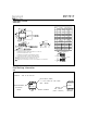

IRF7317
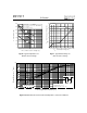
Surface mounted on FR-4 board, t ≤ 10sec.
Parameter Min. Typ. Max. Units Conditions
N-Ch 20 — — V
GS
= 0V, I
D
= 250µA
P-Ch -20 — — V
GS
= 0V, I
D
= -250µA
N-Ch — 0.027 — Reference to 25°C, I
D
= 1mA
P-Ch — 0.031 — Reference to 25°C, I
D
= -1mA
— 0.023 0.029 V
GS
= 4.5V, I
D
= 6.0A
— 0.030 0.046 V
GS
= 2.7V, I
D
= 5.2A
— 0.049 0.058 V
GS
= -4.5V, I
D
= -2.9A
— 0.082 0.098 V
GS
= -2.7V, I
D
= -1.5A
N-Ch 0.7 — — V
DS
= V
GS
, I
D
= 250µA
P-Ch -0.7 — — V
DS
= V
GS
, I
D
= -250µA
N-Ch — 20 — V
DS
= 10V, I
D
= 6.0A
P-Ch — 5.9 — V
DS
= -10V, I
D
= -1.5A
N-Ch — — 1.0 V
DS
= 16V, V
GS
= 0V
P-Ch — — -1.0 V
DS
= -16V, V
GS
= 0V
N-Ch — — 5.0 V
DS
= 16V, V
GS
= 0V, T
J
= 55°C
P-Ch — — -25 V
DS
= -16V, V
GS
= 0V, T
J
= 55°C
I
GSS
Gate-to-Source Forward Leakage N-P –– — ±100 V
GS
= ±12V
N-Ch — 18 27
P-Ch — 19 29
N-Ch — 2.2 3.3
P-Ch — 4.0 6.1
N-Ch — 6.2 9.3
P-Ch — 7.7 12
N-Ch — 8.1 12
P-Ch — 15 22
N-Ch — 17 25
P-Ch — 40 60
N-Ch — 38 57
P-Ch — 42 63
N-Ch — 31 47
P-Ch — 49 73
N-Ch — 900 —
P-Ch — 780 —
N-Ch — 430 — pF
P-Ch — 470 —
N-Ch — 200 —
P-Ch — 240 —
V
(BR)DSS
Drain-to-Source Breakdown Voltage
∆V
(BR)DSS
/∆T
J
Breakdown Voltage Temp. Coefficient
R
DS(ON)
Static Drain-to-Source On-Resistance
V
GS(th)
Gate Threshold Voltage
g
fs
Forward Transconductance
I
DSS
Drain-to-Source Leakage Current
Q
g
Total Gate Charge
Q
gs
Gate-to-Source Charge
Q
gd
Gate-to-Drain ("Miller") Charge
t
d(on)
Turn-On Delay Time
t
r
Rise Time
t
d(off)
Turn-Off Delay Time
t
f
Fall Time
C
iss
Input Capacitance
C
oss
Output Capacitance
C
rss
Reverse Transfer Capacitance
Electrical Characteristics @ T
J
= 25°C (unless otherwise specified)
V
V/°C
Ω
V
S
µA
nC
ns
N-Channel
I
D
= 6.0A, V
DS
= 10V, V
GS
= 4.5V
P-Channel
I
D
= -2.9A, V
DS
= -16V, V
GS
= -4.5V
N-Channel
V
DD
= 10V, I
D
= 1.0A, R
G
= 6.0Ω,
R
D
= 10Ω
P-Channel
V
DD
= -10V, I
D
= -2.9A, R
G
= 6.0Ω,
R
D
= 3.4Ω
N-Channel
V
GS
= 0V, V
DS
= 15V, ƒ = 1.0MHz
P-Channel
V
GS
= 0V, V
DS
= -15V, ƒ = 1.0MHz
N-Ch
P-Ch
Parameter Min. Typ. Max. Units Conditions
N-Ch — — 2.5
P-Ch — — -2.5
N-Ch — — 26
P-Ch — — -21
N-Ch — 0.72 1.0 T
J
= 25°C, I
S
= 1.7A, V
GS
= 0V
P-Ch — -0.78 -1.0 T
J
= 25°C, I
S
= -2.9A, V
GS
= 0V
N-Ch — 52 77
P-Ch — 47 71
N-Ch — 58 86
P-Ch — 49 73
Source-Drain Ratings and Characteristics
I
S
Continuous Source Current (Body Diode)
I
SM
Pulsed Source Current (Body Diode)
V
SD
Diode Forward Voltage
t
rr
Reverse Recovery Time
Q
rr
Reverse Recovery Charge
A
V
ns
nC
N-Channel
T
J
= 25°C, I
F
=1.7A, di/dt = 100A/µs
P-Channel
T
J
= 25°C, I
F
= -2.9A, di/dt = 100A/µs
N-Channel I
SD
≤ 4.1A, di/dt ≤ 92A/µs, V
DD
≤ V
(BR)DSS
, T
J
≤ 150°C
P-Channel I
SD
≤ -2.9A, di/dt ≤ -77A/µs, V
DD
≤ V
(BR)DSS
, T
J
≤ 150°C
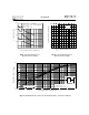
Repetitive rating; pulse width limited by
max. junction temperature. ( See fig. 22 )
Notes:
Pulse width ≤ 300µs; duty cycle ≤ 2%.
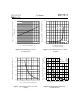
N-Channel Starting T
J
= 25°C, L = 12mH R
G
= 25Ω, I
AS
= 4.1A. (See Figure 12)
P-Channel Starting T
J
= 25°C, L = 35mH R
G
= 25Ω, I
AS
= -2.9A.
nA