
Datasheet

IRF7311
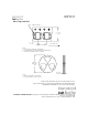
Fig 11. Maximum Effective Transient Thermal Impedance, Junction-to-Ambient
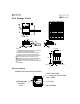
Fig 10. Typical Gate Charge Vs.
Gate-to-Source Voltage
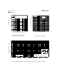
Fig 9. Typical Capacitance Vs.
Drain-to-Source Voltage
0
400
800
1200
1600
1 10 100
C, Capacitance (pF)
DS
V , Drain-to-Source Volta
g
e
(
V
)
A
V = 0V, f = 1MHz
C = C + C , C SHORTED
C = C
C = C + C
GS
iss
g
s
g
d ds
rss
g
d
oss ds
g
d
C
iss
C
oss
C
rss
0 5 10 15 20 25 30
0
2
4
6
8
10
Q , Total Gate Char
g
e (nC)
-V , Gate-to-Source Voltage (V)
G
GS
I =
D
6.0A
V = 10V
DS
0.1
1
10
100
0.00001 0.0001 0.001 0.01 0.1 1 10 100
Notes:
1. Duty factor D = t / t
2. Peak T = P x Z + T
1 2
J DM thJA A
P
t
t
DM
1
2
t , Rectangular Pulse Duration (sec)
Thermal Response (Z )
1
thJA
0.01
0.02
0.05
0.10
0.20
0.50
SINGLE PULSE
(THERMAL RESPONSE)