
Datasheet

154
IRF7309
P-Channel
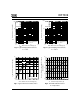
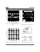
Fig 22b. Gate Charge Test Circuit Fig 22b. Basic Gate Charge Waveform
N- and P-Channel
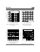
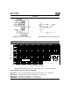
Fig 23. Maximum Effective Transient Thermal Impedance, Junction-to-Ambient
0.1
1
10
100
0.00001 0.0001 0.001 0.01 0.1 1 10 100 1000
t , Rectangular Pulse Duration (sec)
1
D = 0.50
0.01
0.02
0.05
0.10
0.20
SINGLE PULSE
(THERMAL RESPONSE)
A
Thermal Response (Z )
thJA
P
t
2
1
t
DM
Notes:
1. Duty factor D = t / t
2. Peak T = P x Z + T
1 2
J
DM
thJA
A
Refer to the Appendix Section for the following:
Appendix A: Figure 24, Peak Diode Recovery dv/dt Test Circuit — See page 329.
Appendix B: Package Outline Mechanical Drawing — See page 332.
Appendix C: Part Marking Information — See page 332.
Appendix D: Tape and Reel Information — See page 336.