
Datasheet
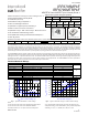

IRF6795MTRPbF
www.irf.com 3
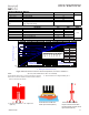
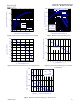
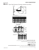
Fig 3. Maximum Effective Transient Thermal Impedance, Junction-to-Ambient
(At lower pulse widths Zth
JA
& Zth
JC
are combined)
Used double sided cooling , mounting pad with large heatsink.
Mounted on minimum footprint full size board with metalized
back and with small clip heatsink.
Notes:
R
θ
is measured at T
J
of approximately 90°C.
Surface mounted on 1 in. square Cu
(still air).
Mounted to a PCB with
small clip heatsink (still air)
Mounted on minimum
footprint full size board with
metalized back and with small
clip heatsink (still air)
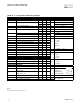
Absolute Maximum Ratin
g
s
Parameter Units
P
D
@T
A
= 25°C Power Dissipation W
P
D
@T
A
= 70°C Power Dissipation
P
D
@T
C
= 25°C Power Dissipation
T
P
Peak Soldering Temperature °C
T
J
Operating Junction and
T
STG
Storage Temperature Range
Thermal Resistance
Parameter Typ. Max. Units
R
θJA
Junction-to-Ambient ––– 45
R
θJA
Junction-to-Ambient 12.5 –––
R
θJA
Junction-to-Ambient 20 ––– °C/W
R
θJC
Junction-to-Case ––– 1.66
R
θJ-PCB
Junction-to-PCB Mounted 1.0 –––
Linear Derating Factor
W/°C
0.022
270
-40 to + 150
Max.
75
2.8
1.8
1E-006 1E-005 0.0001 0.001 0.01 0.1 1 10 100 1000
t
1
, Rectangular Pulse Duration (sec)
0.01
0.1
1
10
100
T
h
e
r
m
a
l
R
e
s
p
o
n
s
e
(
Z
t
h
J
A
)
0.20
0.10
D = 0.50
0.02
0.01
0.05
SINGLE PULSE
( THERMAL RESPONSE )
Notes:
1. Duty Factor D = t1/t2
2. Peak Tj = P dm x Zthja + Tc
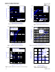
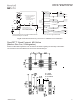
τ
J
τ
J
τ
1
τ
1
τ
2
τ
2
τ
3
τ
3
R
1
R
1
R
2
R
2
R
3
R
3
Ci= τi /Ri
Ci= τi/Ri
τ
4
τ
4
R
4
R
4
τ
A
τ
A
R
8
R
8
τ
5
τ
5
R
5
R
5
τ
6
τ
6
R
6
R
6
τ
7
τ
7
R
7
R
7
Ri (°C/W) τi (sec)
1.64e-02 1.01e-06
2.21e-02 6.00e-06
2.30e-01 8.20e-05
8.64e-01 1.56e-03
1.66e+00 3.96e-03
4.90e-01 6.48e-03
2.37e+01 1.03e+00
1.80e+01 3.98e+01