
Datasheet


IRF6710S2TR/TR1PbF
www.irf.com 7
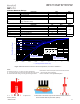
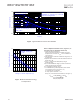
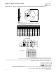
Fig 18a. Gate Charge Test Circuit
Fig 18b. Gate Charge Waveform
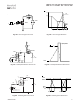
Fig 19b. Unclamped Inductive Waveforms
Fig 19a. Unclamped Inductive Test Circuit
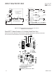
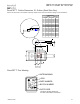
Fig 20b. Switching Time Waveforms
Fig 20a. Switching Time Test Circuit
1K
VCC
DUT
0
L
S
20K
Vds
Vgs
Id
Vgs(th)
Qgs1
Qgs2QgdQgodr
R
G
I
AS
0.01
Ω
t
p
D.U.T
L
V
DS
+
-
V
DD
DRIVER
A
15V
20V
t
p
V
(BR)DSS
I
AS
V
DS
Pulse Width ≤ 1 µs
Duty Factor ≤ 0.1 %
R
D
V
GS
R
G
D.U.T.
10V
+
-
V
DD
V
GS
V
DS
V
GS
90%
10%
t
d(off)
t
d(on)
t
f
t
r