
Datasheet


IRF6710S2TR/TR1PbF
www.irf.com 3
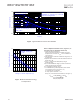
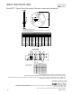
Fig 3. Maximum Effective Transient Thermal Impedance, Junction-to-Ambient
1E-006 1E-005 0.0001 0.001 0.01 0.1 1 10 100
t
1
, Rectangular Pulse Duration (sec)
0.01
0.1
1
10
100
T
h
e
r
m
a
l
R
e
s
p
o
n
s
e
(
Z
t
h
J
A
)
0.20
0.10
D = 0.50
0.02
0.01
0.05
SINGLE PULSE
( THERMAL RESPONSE )
Notes:
1. Duty Factor D = t1/t2
2. Peak Tj = P dm x Zthja + Tc
Ri (°C/W)
τι
(sec)
11.759 0.009459
48.48669 0.9378
21.76032 37.2
τ
J
τ
J
τ
1
τ
1
τ
2
τ
2
τ
3
τ
3
R
1
R
1
R
2
R
2
R
3
R
3
τ
τ
C
Ci= τi/Ri
Ci= τi/Ri
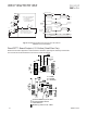
Surface mounted on 1 in. square Cu board, steady state.
T
C
measured with thermocouple incontact with top (Drain) of part.
Used double sided cooling, mounting pad with large heatsink.
Notes:
Mounted on minimum footprint full size board with metalized
back and with small clip heatsink.
R
θ
is measured at T
J
of approximately 90°C.
Surface mounted on 1 in. square Cu
board (still air).
Mounted on minimum footprint full size board with metalized
back and with small clip heatsink. (still air)
Absolute Maximum Ratin
g
s
Parameter Units
P
D
@T
A
= 25°C
Power Dissipation
W
P
D
@T
A
= 70°C
Power Dissipation
P
D
@T
C
= 25°C
Power Dissipation
T
P
Peak Soldering Temperature °C
T
J
Operating Junction and
T
STG
Storage Temperature Range
Thermal Resistance
Parameter Typ. Max. Units
R
θJA
Junction-to-Ambient ––– 82
R
θJA
Junction-to-Ambient 12.5 –––
R
θJA
Junction-to-Ambient 20 ––– °C/W
R
θJC
Junction-to-Case ––– 9.8
R
θJ-PCB
Junction-to-PCB Mounted 1.0 –––
Linear Derating Factor
W/°C
0.012
270
-55 to + 175
Max.
15
1.8
1.3