
Datasheet


www.irf.com 7
IRF6616PbF
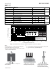
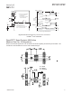
Fig 18. Diode Reverse Recovery Test Circuit for N-Channel
HEXFET
®
Power MOSFETs
P.W.
Period
di/dt
Diode Recovery
dv/dt
Ripple ≤ 5%
Body Diode Forward Drop
Re-Applied
Voltage
Reverse
Recovery
Current
Body Diode Forward
Current
V
GS
=10V
V
DD
I
SD
Driver Gate Drive
D.U.T. I
SD
Waveform
D.U.T. V
DS
Waveform
Inductor Curent
D =
P. W .
Period
* V
GS
= 5V for Logic Level Devices
*
Inductor Current
Circuit Layout Considerations
• Low Stray Inductance
• Ground Plane
• Low Leakage Inductance
Current Transformer
• di/dt controlled by R
G
• Driver same type as D.U.T.
• I
SD
controlled by Duty Factor "D"
• D.U.T. - Device Under Test
+
-
+
+
+
-
-
-
R
G
V
DD
D.U.T
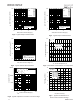
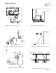
DirectFET Board Footprint, MX Outline
(Medium Size Can, X-Designation).
Please see DirectFET application note AN-1035 for all details regarding the assembly of DirectFET. This
includes all recommendations for stencil and substrate designs.
G = GATE
D = DRAIN
S = SOURCE
D
D
D
D
G
S
S