
Datasheet


IRF6614PbF
6 www.irf.com
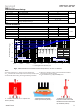
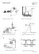
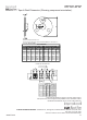
Fig 15a. Gate Charge Test Circuit
Fig 15b. Gate Charge Waveform
Vds
Vgs
Id
Vgs(th)
Qgs1
Qgs2 Qgd Qgodr
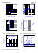
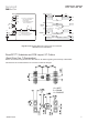
Fig 16c. Unclamped Inductive Waveforms
t
p
V
(BR)DSS
I
AS
Fig 16b. Unclamped Inductive Test Circuit
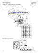
Fig 17b. Switching Time Waveforms
V
GS
V
DS
90%
10%
t
d(on)
t
d(off)
t
r
t
f
Fig 17a. Switching Time Test Circuit
V
GS
Pulse Width < 1µs
Duty Factor < 0.1%
V
DD
V
DS
L
D
D.U.T
+
-
R
G
I
AS
0.01
Ω
t
p
D.U.T
L
V
DS
+
-
V
DD
DRIVER
A
15V
20V
V
GS
1K
VCC
DUT
0
L