
Datasheet


IRF6614PbF
2 www.irf.com
Repetitive rating; pulse width limited by max. junction temperature.
Pulse width ≤ 400µs; duty cycle ≤ 2%.
Notes:
Static @ T
J
= 25°C (unless otherwise specified)
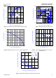
Parameter Min. Typ. Max. Units
BV
DSS
Drain-to-Source Breakdown Voltage
40 ––– ––– V
∆ΒV
DSS
/∆T
J
Breakdown Voltage Temp. Coefficient
––– 38 ––– mV/°C
R
DS(on)
Static Drain-to-Source On-Resistance
––– 5.9 8.3 mΩ
––– 7.1 9.9
V
GS(th)
Gate Threshold Voltage
1.35 1.80 2.25 V
∆V
GS(th)
/∆T
J
Gate Threshold Voltage Coefficient
––– -5.5 ––– mV/°C
I
DSS
Drain-to-Source Leakage Current
––– ––– 1.0 µA
––– ––– 150
I
GSS
Gate-to-Source Forward Leakage
––– ––– 100 nA
Gate-to-Source Reverse Leakage
––– ––– -100
gfs Forward Transconductance
71 ––– ––– S
Q
g
Total Gate Charge
––– 19 29
Q
gs1
Pre-Vth Gate-to-Source Charge
––– 5.9 –––
Q
gs2
Post-Vth Gate-to-Source Charge
––– 1.4 ––– nC
Q
gd
Gate-to-Drain Charge
––– 6.0 –––
Q
godr
Gate Charge Overdrive
––– 5.7 –––
See Fig. 15
Q
sw
Switch Charge (Q
gs2
+ Q
gd
)
––– 7.4 –––
Q
oss
Output Charge
––– 9.5 ––– nC
R
G
Gate Resistance
––– 1.0 1.5
Ω
t
d(on)
Turn-On Delay Time –––
13
–––
t
r
Rise Time –––
27
–––
t
d(off)
Turn-Off Delay Time –––
18
––– ns
t
f
Fall Time –––
3.6
–––
C
iss
Input Capacitance –––
2560
–––
C
oss
Output Capacitance –––
370
––– pF
C
rss
Reverse Transfer Capacitance –––
200
–––
Diode Characteristics
Parameter Min. Typ. Max. Units
I
S
Continuous Source Current
––– ––– 53
(Body Diode) A
I
SM
Pulsed Source Current
––– ––– 102
(Body Diode)g
V
SD
Diode Forward Voltage
––– ––– 1.0
V
t
rr
Reverse Recovery Time
––– 15 23
ns
Q
rr
Reverse Recovery Charge
––– 5.5 8.3
nC
V
DS
= 32V, V
GS
= 0V, T
J
= 125°C
V
GS
= 20V
V
GS
= -20V
V
GS
= 4.5V
I
D
= 10.2A
V
GS
= 0V
V
DS
= 20V
I
D
= 10.2A
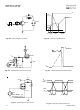
T
J
= 25°C, I
F
= 10.2A
di/dt = 100A/µs i
T
J
= 25°C, I
S
= 10.2A, V
GS
= 0V i
showing the
integral reverse
p-n junction diode.
Conditions
V
GS
= 0V, I
D
= 250µA
Reference to 25°C, I
D
= 1mA
V
GS
= 10V, I
D
= 12.7A i
V
GS
= 4.5V, I
D
= 10.2A i
V
DS
= V
GS
, I
D
= 250µA
V
DS
= 32V, V
GS
= 0V
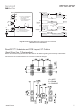
MOSFET symbol
Clamped Inductive Load
V
DS
= 10V, I
D
= 10.2A
Conditions
ƒ = 1.0MHz
V
DS
= 16V, V
GS
= 0V
V
DD
= 20V, V
GS
= 4.5Vi
V
DS
= 20V