
Datasheet

IRF5210S/LPbF
www.irf.com 5
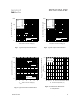
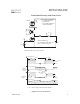
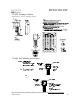
Fig 10a. Switching Time Test Circuit
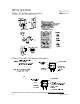
Fig 10b. Switching Time Waveforms
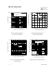
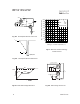
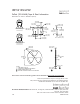
Fig 11. Maximum Effective Transient Thermal Impedance, Junction-to-Case
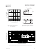
Fig 9. Maximum Drain Current vs.
Case Temperature
V
DS
-10V
Pulse Width ≤ 1 µs
Duty Factor ≤ 0.1 %
R
D
V
GS
V
DD
R
G
D.U.T.
+
-
V
DS
90%
10%
V
GS
t
d(on)
t
r
t
d(off)
t
f
25 50 75 100 125 150
T
C
, Case Temperature (°C)
0
5
10
15
20
25
30
35
40
-
I
D
,
D
r
a
i
n
C
u
r
r
e
n
t
(
A
)
1E-006 1E-005 0.0001 0.001 0.01 0.1 1
t
1
, Rectangular Pulse Duration (sec)
0.001
0.01
0.1
1
T
h
e
r
m
a
l
R
e
s
p
o
n
s
e
(
Z
t
h
J
C
)
0.20
0.10
D = 0.50
0.02
0.01
0.05
SINGLE PULSE
( THERMAL RESPONSE )
Notes:
1. Duty Factor D = t1/t2
2. Peak Tj = P dm x Zthjc + Tc
Ri (°C/W)
τι (sec)
0.128309 0.000069
0.377663 0.001772
0.244513 0.010024
τ
J
τ
J
τ
1
τ
1
τ
2
τ
2
τ
3
τ
3
R
1
R
1
R
2
R
2
R
3
R
3
τ
τ
C
Ci= τi/Ri
Ci= τi/Ri