
Datasheet


IRF4905S/L
6 www.irf.com
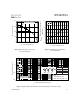
Fig 13b. Gate Charge Test Circuit
Fig 13a. Basic Gate Charge Waveform
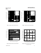
Fig 12c. Maximum Avalanche Energy
Vs. Drain Current
Fig 12b. Unclamped Inductive Waveforms
Fig 12a. Unclamped Inductive Test Circuit
Fig 14. Threshold Voltage Vs. Temperature
25 50 75 100 125 150
Starting T
J
, Junction Temperature (°C)
0
100
200
300
400
500
600
E
A
S
,
S
i
n
g
l
e
P
u
l
s
e
A
v
a
l
a
n
c
h
e
E
n
e
r
g
y
(
m
J
)
I
D
TOP
-17A
-30A
BOTTOM
-42A
-75 -50 -25 0 25 50 75 100 125 150
T
J
, Temperature ( °C )
2.0
2.4
2.8
3.2
3.6
-
V
G
S
(
t
h
)
G
a
t
e
t
h
r
e
s
h
o
l
d
V
o
l
t
a
g
e
(
V
)
I
D
= -250µA
D.U.T.
V
DS
I
D
I
G
-3mA
V
GS
.3µF
50KΩ
.2µF
12V
Current Regulator
Same Type as D.U.T.
Current Sampling Resistors
+
-
Q
G
Q
GS
Q
GD
V
G
Charge
10V
t
p
V
(
BR
)
DSS
I
AS
R
G
I
AS
0.01
Ω
t
p
D.U.T
L
V
DS
V
DD
DRIVER
A
15V
-20V