
Datasheet

IRF3709Z/S/LPbF
6 www.irf.com
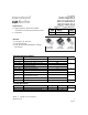
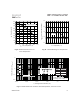
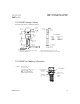
Fig 13. On-Resistance vs. Gate Voltage
Fig 12. On-Resistance vs. Drain Current
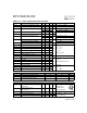
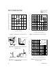
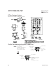
Fig 16. Maximum Avalanche Energy
vs. Drain Current
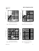
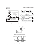
Fig 14a&b. Basic Gate Charge Test Circuit
and Waveform
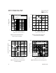
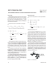
Fig 15a&b. Unclamped Inductive Test circuit
and Waveforms
t
p
V
(BR)DSS
I
AS
R
G
I
AS
0.01
Ω
t
p
D.U.T
L
V
DS
+
-
V
DD
DRIVER
A
15V
20V
D.U.T.
V
DS
I
D
I
G
3mA
V
GS
.3µF
50KΩ
.2µF
12V
Current Regulator
Same Type as D.U.T.
Current Sampling Resistors
+
-
Vds
Vgs
Id
Vgs(th)
Qgs1
Qgs2 Qgd Qgodr
2 3 4 5 6 7 8 9 10
V
GS,
Gate -to -Source Voltage (V)
0
2
4
6
8
10
12
14
16
R
D
S
(
o
n
)
,
D
r
a
i
n
-
t
o
-
S
o
u
r
c
e
O
n
R
e
s
i
s
t
a
n
c
e
(
m
Ω
)
I
D
= 21A
T
J
= 25°C
T
J
= 125°C
10.0 20.0 30.0 40.0 50.0 60.0 70.0
I
D
, Drain Current (A)
4.00
5.00
6.00
7.00
8.00
9.00
R
D
S
(
o
n
)
,
D
r
a
i
n
-
t
o
-
S
o
u
r
c
e
O
n
R
e
s
i
s
t
a
n
c
e
(
m
Ω
)
T
J
= 25°C
T
J
= 125°C
Vgs = 10V
25 50 75 100 125 150 175
Starting T
J
, Junction Temperature (°C)
0
50
100
150
200
250
E
A
S
,
S
i
n
g
l
e
P
u
l
s
e
A
v
a
l
a
n
c
h
e
E
n
e
r
g
y
(
m
J
)
I
D
TOP 5.4A
8.0A
BOTTOM 17A