
Datasheet

IRF3205ZS/L
6 www.irf.com
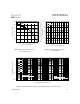
Q
G
Q
GS
Q
GD
V
G
Charge
10 V
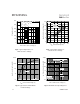
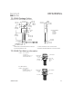
Fig 13b. Gate Charge Test Circuit
Fig 13a. Basic Gate Charge Waveform
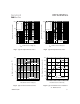
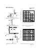
Fig 12c. Maximum Avalanche Energy
Vs. Drain Current
Fig 12b. Unclamped Inductive Waveforms
Fig 12a. Unclamped Inductive Test Circuit
t
p
V
(BR)DSS
I
AS
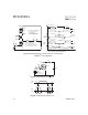
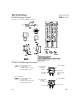
Fig 14. Threshold Voltage Vs. Temperature
R
G
I
AS
0.01
Ω
t
p
D.U.T
L
V
DS
+
-
V
DD
DRIVER
A
15V
20V
V
GS
25 50 75 100 125 150 175
Starting T
J
, Junction Temperature (°C)
0
50
100
150
200
250
300
350
E
A
S
,
S
i
n
g
l
e
P
u
l
s
e
A
v
a
l
a
n
c
h
e
E
n
e
r
g
y
(
m
J
)
I
D
TOP 27A
47A
BOTTOM 66A
-75 -50 -25 0 25 50 75 100 125 150 175
T
J
, Temperature ( °C )
1.0
2.0
3.0
4.0
V
G
S
(
t
h
)
G
a
t
e
t
h
r
e
s
h
o
l
d
V
o
l
t
a
g
e
(
V
)
I
D
= 250µA
1K
VCC
DUT
0
L