
Datasheet

IRF2907ZS-7PPbF
2 www.irf.com
Notes:
Repetitive rating; pulse width limited by
max. junction temperature. (See fig. 11).
Limited by T
Jmax
, starting T
J
= 25°C,
L=0.026mH, R
G
= 25Ω, I
AS
= 110A, V
GS
=10V.
Part not recommended for use above this value.
Pulse width ≤ 1.0ms; duty cycle ≤ 2%.
C
oss
eff. is a fixed capacitance that gives the same
charging time as C
oss
while V
DS
is rising from 0 to 80%
V
DSS
.
Limited by T
Jmax
, see Fig.12a, 12b, 15, 16 for typical repetitive
avalanche performance.
This value determined from sample failure population. 100%
tested to this value in production.
This is applied to D
2
Pak, when mounted on 1" square PCB
( FR-4 or G-10 Material ). For recommended footprint and
soldering techniques refer to application note #AN-994.
R
θ
is measured at T
J
of approximately 90°C.
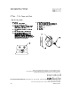
S
D
G
S
D
G
Static @ T
J
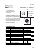
= 25°C (unless otherwise specified)
Parameter Min. T
y
p. Max. Units
V
(BR)DSS
Drain-to-Source Breakdown Volta
g
e75––––––V
∆Β
V
DSS
/
∆
T
J
Breakdown Volta
g
e Temp. Coefficient ––– 0.066 ––– V/°C
R
DS(on)
SMD
Static Drain-to-Source On-Resistance –––
3.0 3.8
mΩ
V
GS(th)
Gate Threshold Volta
g
e 2.0 ––– 4.0 V
g
fs
Forward Transconductance
94 ––– ––– S
I
DSS
Drain-to-Source Leaka
g
e Current ––– ––– 20
µ
A
––– ––– 250
I
GSS
Gate-to-Source Forward Leaka
g
e ––– ––– 200 nA
Gate-to-Source Reverse Leaka
g
e ––– ––– -200
Q
g
Total Gate Char
g
e ––– 170 260 nC
Q
gs
Gate-to-Source Char
g
e ––– 55 –––
Q
gd
Gate-to-Drain ("Miller") Char
g
e ––– 66 –––
t
d(on)
Turn-On Dela
y
Time ––– 21 ––– ns
t
r
Rise Time ––– 90 –––
t
d(off)
Turn-Off Dela
y
Time ––– 92 –––
t
f
Fall Time ––– 44 –––
L
D
Internal Drain Inductance ––– 4.5 ––– nH Between lead,
6mm (0.25in.)
L
S
Internal Source Inductance ––– 7.5 ––– from packa
g
e
and center of die contact
C
iss
Input Capacitance ––– 7580 ––– pF
C
oss
Output Capacitance ––– 970 –––
C
rss
Reverse Transfer Capacitance ––– 540 –––
C
oss
Output Capacitance ––– 3750 –––
C
oss
Output Capacitance ––– 650 –––
C
oss
eff.
Effective Output Capacitance ––– 1110 –––
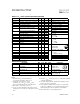
Diode Characteristics
Parameter Min. T
y
p. Max. Units
I
S
Continuous Source Current ––– ––– 160
(Body Diode) A
I
SM
Pulsed Source Current ––– ––– 700
(Body Diode)
V
SD
Diode Forward Voltage
––– ––– 1.3 V
t
rr
Reverse Recovery Time
–––3553ns
Q
rr
Reverse Recover
y
Char
g
e ––– 40 60 nC
V
DS
= V
GS
, I
D
= 250µA
V
DS
= 75V, V
GS
= 0V
V
DS
= 75V, V
GS
= 0V, T
J
= 125°C
Conditions
V
GS
= 0V, I
D
= 250µA
Reference to 25°C, I
D
= 1mA
V
GS
= 10V, I
D
= 110A
T
J
= 25°C, I
F
= 110A, V
DD
= 38V
di/dt = 100A/
µ
s
T
J
= 25°C, I
S
= 110A, V
GS
= 0V
showing the
integral reverse
p-n junction diode.
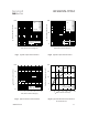
V
GS
= 0V, V
DS
= 1.0V, ƒ = 1.0MHz
V
GS
= 10V
MOSFET symbol
V
GS
= 0V
V
DS
= 25V
V
GS
= 0V, V
DS
= 60V, ƒ = 1.0MHz
Conditions
V
GS
= 0V, V
DS
= 0V to 60V
ƒ = 1.0MHz, See Fig. 5
R
G
= 2.6Ω
I
D
= 110A
V
DS
= 25V, I
D
= 110A
V
DD
= 38V
I
D
= 110A
V
GS
= 20V
V
GS
= -20V
V
DS
= 60V
V
GS
= 10V