
Datasheet

IRF2907Z/S/LPbF
6 www.irf.com
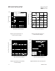
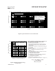
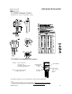
Q
G
Q
GS
Q
GD
V
G
Charge
10 V
Fig 13b. Gate Charge Test Circuit
Fig 13a. Basic Gate Charge Waveform
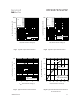
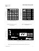
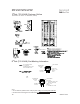
Fig 12c. Maximum Avalanche Energy
vs. Drain Current
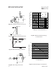
Fig 12b. Unclamped Inductive Waveforms
Fig 12a. Unclamped Inductive Test Circuit
t
p
V
(BR)DSS
I
AS
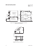
Fig 14. Threshold Voltage vs. Temperature
R
G
I
AS
0.01
Ω
t
p
D.U.T
L
V
DS
+
-
V
DD
DRIVER
A
15V
20V
V
GS
1K
VCC
DUT
0
L
-75 -50 -25 0 25 50 75 100 125 150 175 200
T
J
, Temperature ( °C )
1.0
1.5
2.0
2.5
3.0
3.5
4.0
V
G
S
(
t
h
)
G
a
t
e
t
h
r
e
s
h
o
l
d
V
o
l
t
a
g
e
(
V
)
I
D
= 250µA
25 50 75 100 125 150 175
Starting T
J
, Junction Temperature (°C)
0
200
400
600
800
1000
1200
E
A
S
,
S
i
n
g
l
e
P
u
l
s
e
A
v
a
l
a
n
c
h
e
E
n
e
r
g
y
(
m
J
)
I
D
TOP 9.0A
13A
BOTTOM 75A