
Datasheet

IRF2804S-7PPbF
6 www.irf.com
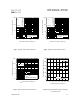
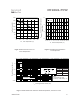
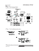
Q
G
Q
GS
Q
GD
V
G
Charge
10 V
Fig 13b. Gate Charge Test Circuit
Fig 13a. Basic Gate Charge Waveform
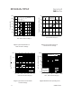
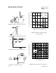
Fig 12c. Maximum Avalanche Energy
vs. Drain Current
Fig 12b. Unclamped Inductive Waveforms
Fig 12a. Unclamped Inductive Test Circuit
t
p
V
(BR)DSS
I
AS
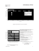
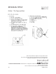
Fig 14. Threshold Voltage vs. Temperature
R
G
I
AS
0.01
Ω
t
p
D.U.T
L
V
DS
+
-
V
DD
DRIVER
A
15V
20V
V
GS
1K
VCC
DUT
0
L
25 50 75 100 125 150 175
Starting T
J
, Junction Temperature (°C)
0
500
1000
1500
2000
2500
E
A
S
,
S
i
n
g
l
e
P
u
l
s
e
A
v
a
l
a
n
c
h
e
E
n
e
r
g
y
(
m
J
)
I
D
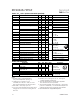
TOP 21A
33A
BOTTOM 160A
-75 -50 -25 0 25 50 75 100 125 150 175
T
J
, Temperature ( °C )
0.5
1.0
1.5
2.0
2.5
3.0
3.5
4.0
4.5
V
G
S
(
t
h
)
G
a
t
e
t
h
r
e
s
h
o
l
d
V
o
l
t
a
g
e
(
V
)
I
D
= 1.0A
I
D
= 1.0mA
I
D
= 250µA