
Datasheet

IRF1405PbF
2 www.irf.com
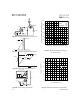
Repetitive rating; pulse width limited by
max. junction temperature. (See fig. 11).
Starting T
J
= 25°C, L = 0.11mH
R
G
= 25Ω, I
AS
= 101A. (See Figure 12).
I
SD
≤ 101A, di/dt ≤ 210A/µs, V
DD
≤ V
(BR)DSS
,
T
J
≤ 175°C
Pulse width ≤ 400µs; duty cycle ≤ 2%.
Notes:
C
oss
eff. is a fixed capacitance that gives the same charging time
as C
oss
while V
DS
is rising from 0 to 80% V
DSS
.
Calculated continuous current based on maximum allowable
junction temperature. Package limitation current is 75A.
Limited by T
Jmax
, see Fig.12a, 12b, 15, 16 for typical repetitive
avalanche performance.
S
D
G
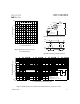
Electrical Characteristics @ TJ = 25°C (unless otherwise specified)
Parameter Min. Typ. Max. Units
V
(BR)DSS
Drain-to-Source Breakdown Voltage 55 ––– ––– V
∆V
(
BR
)
DSS
/∆T
J
Breakdown Voltage Temp. Coefficient ––– 0.057 ––– V/°C
R
DS(on)
Static Drain-to-Source On-Resistance ––– 4.6 5.3
mΩ
V
GS(th)
Gate Threshold Voltage 2.0 ––– 4.0 V
gfs Forward Transconductance 69 ––– ––– S
I
DSS
Drain-to-Source Leakage Current ––– ––– 20 µA
––– ––– 250
I
GSS
Gate-to-Source Forward Leakage ––– ––– 200 nA
Gate-to-Source Reverse Leakage ––– ––– -200
Q
g
Total Gate Charge ––– 170 260
Q
gs
Gate-to-Source Charge ––– 44 66 nC
Q
gd
Gate-to-Drain ("Miller") Charge ––– 62 93
t
d(on)
Turn-On Delay Time ––– 13 –––
t
r
Rise Time ––– 190 –––
t
d(off)
Turn-Off Delay Time ––– 130 ––– ns
t
f
Fall Time ––– 110 –––
L
D
Internal Drain Inductance Between lead,
nH 6mm (0.25in.)
L
S
Internal Source Inductance from package
and center of die contact
C
iss
Input Capacitance ––– 5480 –––
C
oss
Output Capacitance ––– 1210 –––
C
rss
Reverse Transfer Capacitance ––– 280 ––– pF
C
oss
Output Capacitance ––– 5210 –––
C
oss
Output Capacitance ––– 900 –––
C
oss
eff.
Effective Output Capacitance
–––1500–––
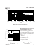
Source-Drain Ratin
g
s and Characteristics
Parameter Min. Typ. Max. Units
I
S
Continuous Source Current
(Body Diode) A
I
SM
Pulsed Source Current
(Body Diode)
V
SD
Diode Forward Voltage ––– ––– 1.3 V
t
rr
Reverse Recovery Time ––– 88 130 ns
Q
rr
Reverse Recovery Charge ––– 250 380 nC
t
on
Forward Turn-On Time
––– ––– 169
––– ––– 680
4.5–––
–––
–––
–––7.5
Intrinsic turn-on time is negligible (turn-on is dominated by LS+LD)
V
DS
= 25V, I
D
= 101A
I
D
= 101A
V
DS
= 44V
Conditions
V
GS
= 10V
V
GS
= 0V
V
DS
= 25V
ƒ = 1.0MHz, See Fig.5
V
GS
= 20V
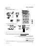
MOSFET symbol
showing the
integral reverse
V
GS
= 0V, V
DS
= 44V, ƒ = 1.0MHz
V
GS
= 0V, V
DS
= 0V to 44V
p-n junction diode.
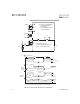
T
J
= 25°C, I
S
= 101A, V
GS
= 0V
T
J
= 25°C, I
F
= 101A
di/dt = 100A/µs
Conditions
V
GS
= 0V, I
D
= 250µA
Reference to 25°C, I
D
= 1mA
V
GS
= 10V, I
D
= 101A
V
DS
= V
GS
, I
D
= 250µA
V
DS
= 55V, V
GS
= 0V
V
DS
= 44V, V
GS
= 0V, T
J
= 150°C
V
GS
= 0V, V
DS
= 1.0V, ƒ = 1.0MHz
V
GS
= 10V
V
DD
= 38V
I
D
= 101A
R
G
= 1.1
Ω
V
GS
= -20V