
Datasheet

IRF1404S/LPbF
2 www.irf.com
Electrical Characteristics @ T
J
= 25°C (unless otherwise specified)
Repetitive rating; pulse width limited by
max. junction temperature. (See fig. 11)
I
SD
≤ 95A, di/dt ≤ 150A/µs, V
DD
≤ V
(BR)DSS
,
T
J
≤ 175°C
Notes:
Starting T
J
= 25°C, L = 0.12mH
R
G
= 25Ω, I
AS
= 95A. (See Figure 12)
Pulse width ≤ 300µs; duty cycle ≤ 2%.
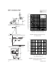
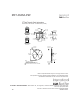
S
D
G
Parameter Min. Typ. Max. Units Conditions
I
S
Continuous Source Current MOSFET symbol
(Body Diode)
––– –––
showing the
I
SM
Pulsed Source Current integral reverse
(Body Diode)
––– –––
p-n junction diode.
V
SD
Diode Forward Voltage ––– ––– 1.3 V T
J
= 25°C, I
S
= 95A, V
GS
= 0V
t
rr
Reverse Recovery Time ––– 71 110 ns T
J
= 25°C, I
F
= 95A
Q
rr
Reverse RecoveryCharge ––– 180 270 nC di/dt = 100A/µs
t
on
Forward Turn-On Time Intrinsic turn-on time is negligible (turn-on is dominated by L
S
+L
D
)
Source-Drain Ratings and Characteristics
162
650
A
C
oss
eff. is a fixed capacitance that gives the same charging time
as C
oss
while V
DS
is rising from 0 to 80% V
DSS
Calculated continuous current based on maximum allowable
junction temperature. Package limitation current is 75A
Parameter Min. Typ. Max. Units Conditions
V
(BR)DSS
Drain-to-Source Breakdown Voltage 40 ––– ––– V V
GS
= 0V, I
D
= 250µA
∆V
(BR)DSS
/∆T
J
Breakdown Voltage Temp. Coefficient ––– 0.036 ––– V/°C Reference to 25°C, I
D
= 1mA
R
DS(on)
Static Drain-to-Source On-Resistance ––– 0.00350.004 Ω V
GS
= 10V, I
D
= 95A
V
GS(th)
Gate Threshold Voltage 2.0 ––– 4.0 V V
DS
= 10V, I
D
= 250µA
g
fs
Forward Transconductance 106 ––– ––– S V
DS
= 25V, I
D
= 60A
––– ––– 20
µA
V
DS
= 40V, V
GS
= 0V
––– ––– 250 V
DS
= 32V, V
GS
= 0V, T
J
= 150°C
Gate-to-Source Forward Leakage ––– ––– 200 V
GS
= 20V
Gate-to-Source Reverse Leakage ––– ––– -200
nA
V
GS
= -20V
Q
g
Total Gate Charge ––– 160 200 I
D
= 95A
Q
gs
Gate-to-Source Charge ––– 35 ––– nC V
DS
= 32V
Q
gd
Gate-to-Drain ("Miller") Charge ––– 42 60 V
GS
= 10V
t
d(on)
Turn-On Delay Time ––– 17 ––– V
DD
= 20V
t
r
Rise Time ––– 140 ––– I
D
= 95A
t
d(off)
Turn-Off Delay Time ––– 72 ––– R
G
= 2.5Ω
t
f
Fall Time ––– 26 ––– R
D
= 0.21Ω
Between lead,
and center of die contact
C
iss
Input Capacitance ––– 7360 ––– V
GS
= 0V
C
oss
Output Capacitance ––– 1680 ––– V
DS
= 25V
C
rss
Reverse Transfer Capacitance ––– 240 ––– pF ƒ = 1.0MHz, See Fig. 5
C
oss
Output Capacitance ––– 6630 ––– V
GS
= 0V, V
DS
= 1.0V, ƒ = 1.0MHz
C
oss
Output Capacitance ––– 1490 ––– V
GS
= 0V, V
DS
= 32V, ƒ = 1.0MHz
C
oss
eff. Effective Output Capacitance ––– 1540 ––– V
GS
= 0V, V
DS
= 0V to 32V
I
GSS
ns
I
DSS
Drain-to-Source Leakage Current
nH
7.5
L
S
Internal Source Inductance
–––
–––
Use IRF1404 data and test conditions.
* When mounted on 1" square PCB ( FR-4 or G-10 Material ).
For recommended footprint and soldering techniques refer to application note #AN-994.