
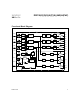
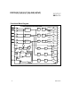
Datasheet


www.irf.com 5
IR2136(2)(3)(5)(6)(7)(8)
(
J&S) & (PbF
)
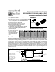
VCC VBS ITRIP ENABLE FAULT LO1,2,3 HO1,2,3
<UVCC X X X 0 (note 1) 0 0
15V <UVBS 0V 5V high imp LIN1,2,3 0
15V 15V 0V 5V high imp LIN1,2,3 HIN1,2,3
15V 15V >V
ITRIP
5V 0 (note 2) 0 0
15V 15V 0V 0V high imp 0 0
Note: A shoot-through prevention logic prevents LO1,2,3 and HO1,2,3 for each channel from turning on simultaneously.
Note 1: UVCC is not latched, when VCC>UVCC, FAULT returns to high impedance.
Note 2: When ITRIP <V
ITRIP
, FAULT returns to high-impedance after RCIN pin becomes greater than 8V (@ VCC = 15V)
NOTE: For high side PWM, HIN pulse width must be ≥ 1µsec
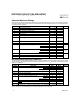
Dynamic Electrical Characteristics
V
CC
= V
BS
= V
BIAS
= 15V, V
S1,2,3
= V
SS
= COM, TA = 25
o
C and C
L
= 1000 pF unless otherwise specified.
Symbol Definition Min. Typ. Max. Units Test Conditions
t
on
Turn-on propagation delay IR2136(2)(3)(5)(8) 300 425 550
IR21366(7) — 250 —
t
off
Turn-off propagation delay IR2136(2)(3)(5)(8) 250 400 550
IR21366(7) — 180 —
t
r
Turn-on rise time — 125 190
t
f
Turn-off fall time — 50 75
t
EN
ENABLE low to output IR2136(2)(3)(5)(8) 300 450 600 V
IN,
V
EN
= 0V or 5V
shutdown propagation delay IR21366(7) 100 250 400
t
ITRIP
ITRIP to output shutdown propagation delay 500 750 1000 V
ITRIP
= 5V
t
bl
ITRIP blanking time 100 150 — V
IN
= 0V or 5V
V
ITRIP
= 5V
t
FLT
ITRIP to FAULT propagation delay 400 600 800 V
IN
= 0V or 5V
V
ITRIP
= 5V
t
FILIN
Input filter time (HIN, LIN, EN) 100 200 — V
IN
= 0 & 5V
(IR2136(2)(3)(5)(8) only)
t
FLTCLR
FAULT clear time RCIN: R=2meg, C=1nF 1.3 1.65 2 mS V
IN
= 0V or 5V
V
ITRIP
= 0V
DT Deadtime 220 290 360 V
IN
= 0 & 5V
MT Matching delay ON and OFF — 40 75
MDT Matching delay, max (t
on
,t
off
) - min (t
on
,t
off
), — 25 70
(ton,toff are applicable to all 3 channels)
PM Output pulse width matching, PWin -PWout (fig.2) — 40 75
nS
V
IN
= 0 & 5V
nS
External dead
time
>400nsec