
Datasheet


www.irf.com 3
IR2136(2)(3)(5)(6)(7)(8)
(
J&S) & (PbF
)
Note 2: All input pins and the ITRIP pin are internally clamped with a 5.2V zener diode.
Recommended Operating Conditions cont.
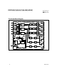
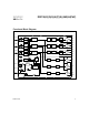
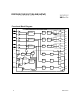
The Input/Output logic timing diagram is shown in figure 1. For proper operation the device should be used within the recom-
mended conditions. All voltage parameters are absolute referenced to COM. The V
S
offset rating is tested with all supplies
biased at 15V differential.
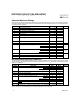
Symbol Definition Min. Max. Units
V
Static Electrical Characteristics
V
BIAS
(V
CC
, V
BS
1,2,3) = 15V unless otherwise specified. The V
IN
, V
TH
and I
IN
parameters are referenced to V
SS
and
are applicable to all six channels (H
S
1,2,3 and L
S
1,2,3). The V
O
and I
O
parameters are referenced to COM and V
S
1,2,3
and are applicable to the respective output leads: H
O1,2,3
and L
O1,2,3.
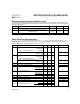
Symbol Definition Min. Typ. Max. Units Test Conditions
V
IH
Logic “0” input voltage LIN1,2,3, HIN1,2,3
IR2136(3)(5) 3.0 — —
Logic “1” input voltage HIN1,2,3 IR21362
Logic “0” input voltage LIN1,2,3, HIN1,2,3
IR21366(7)(8) 2.5 — —
V
IL
Logic “1” input voltage LIN1,2,3, HIN1,2,3
IR2136(3)(5) — — 0.8
Logic “0” input voltage HIN1,2,3 IR21362
Logic “0” input voltage LIN1,2,3, HIN1,2,3
IR21366(7)(8) — — 0.8
V
EN,TH+
EN positive going threshold — — 3
V
EN,TH-
EN negative going threshold 0.8 — —
V
IT,TH+
ITRIP positive going threshold
IR2136(2)(3)(6) 0.37 0.46 0.55
IR21365(7)(8) 3.85 4.30 4.75
V
IT,HYS
ITRIP input hysteresis
IR2136(2)(3)(6) — 0.07 —
IR21365(7)(8) — .15 —
V
RCIN,TH+
RCIN positive going threshold — 8 —
V
RCIN,HYS
RCIN input hysteresis — 3 —
V
OH
High level output voltage, V
BIAS
- V
O
— 0.9 1.4 I
O
= 20 mA
V
OL
Low level output voltage, V
O
— 0.4 0.6 I
O
= 20 mA
V
CCUV+
V
CC
and V
BS
supply undervoltage IR2136(8) 8.0 8.9 9.8
V
BSUV+
positive going threshold IR21362 9.6 10.4 11.2
IR21363(5)(6)(7) 10.6 11.1 11.6
V
V
ITRIP
ITRIP input voltage V
SS
V
SS
+5
V
IN
Logic input voltage , HIN (IR2136,IR21363(5)(6)(7)(8)),
HIN(IR21362), EN V
SS
V
SS
+5
T
A
Ambient temperature -40 125
o
C